The microcomputers must be able to communicate with external peripherals. This is possible thanks to buffers allowing the microprocessor to control a much larger number of circuits than that which it is capable of driving alone.
These buffers receive certain control signals from other circuits of the Computer which, in this experiment, will be simulated. In the next chapters, you will see the characteristics of these control signals and how they are generated. For now, you will check that the buffers work.
The buffer that will be examined first, the 74LS243, is of a particular type ; it is called in English transceiver (contraction of transmitter and receiver), that is to say transmetteur and récepteur.
Indeed, this buffer is bidirectional ; this means that the inputs can become the outputs and vice versa via a signal applied to a control input.
The integrated circuit 74LS243 contains four bidirectional buffers ; the Figure 7-a represents only one of them.
One can see in the equivalent circuit of the Figure 7-b that the signal can go One can see in the equivalent circuit of the figure 7-b that the signal can go from A towards B in the branch containing the contact 1 or of B towards A in that containing the contact 2.
Terminals A and B can operate as inputs or as outputs ; they constitute the inputs / outputs of two Schmitt triggers which can be set to the high impedance state, like the integrated circuit 74LS125 used in the previous practice.
The operation of the circuit is controlled by the inputs AB
and GBA which can put the triggers in the high impedance state if they are activated.
The principle is simple : when we want to transmit the signal from A to B, we act on the control inputs AB
and GBA so that trigger 1 is validated and the other is in the high impedance state.
Referring to the equivalent circuit of the Figure 7-b, it is as if contact 1 was closed and contact 2 open.
When, on the other hand, we want to transmit the signal from B to A, we act on the inputs AB
and GBA so that trigger 1 is in the high impedance state and that trigger 2 is validated.
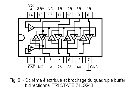
The Figure 8 shows the electrical diagram and pinout of the integrated circuit 74LS243.
FIRST TEST : 74LS243 BUFFER TEST
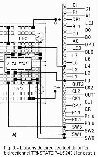
3. 1. - REALIZATION OF THE CIRCUIT (FIGURE 9)
a) Remove from the matrix with contacts all the components and connections relating to the preceding experiment.
b) Insert on the matrix the integrated circuit 74LS243 and its two resistances of 1 kΩ and carry out the connections illustrated Figure 9-a.
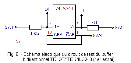
The electric diagram of the circuit carried out is given Figure 9-b.
3. 2. - OPERATION TEST
a) Place the switches SW0, SW1 and SW3 on position 0.
b) Switch on the digilab.
c) Observe the LEDs L0 and L4 : they are off.
d) Switch SW1 several times : you observe that the two LEDs remain off.
You have thus checked that SW1 does not influence the circuit, which shows that SW1 is not connected to an input but to an output.
e) Switch SW0 several times : you observe that the LED L0 lights up and goes out according to the position of SW0 at the same time as the LED L4, which means that SW0 is connected to an input.
f) Now switch to SW1 : you see that it has no influence on the circuit.
You have just checked in practice the hypothesis that terminal 1A is the input of the circuit and terminal 1B the output.
g) Place SW3 on position 1 : you apply a high level on the GBA and AB control inputs.
h) Repeat the previous tests by switching SW0 and SW1 : you notice that, in this case, SW0 no longer has any influence on the circuit while SW1 assumes control of it ; we therefore deduce that terminal 1B has become the input while terminal 1A has become the output.
i) Switch off the digilab.
j) Remove the link between pin 1 and pin 13, connect SW3 to pin 13 and pin 1 (AB)
to the positive voltage (+). Finally place SW3 on position 0.
k) Switch on the digilab : you notice that any switching of SW0 and SW1 is immediately translated by L0 and L4 without influencing the other side of the circuit.
We can therefore say that the buffer plays no role and that everything happens as if SW1 were only in contact with L4 and SW0 with L0.
l) By cutting the power each time, repeat the previous tests for the three other buffers of the integrated circuit ; this will be fully tested.
NOTE :
If one applies to the entry
AB
a low level and to the entry GBA a high level, the two triggers of Schmitt are validated. This operating mode is however not interesting since neither of the two terminals could be considered as input.
m) At the end of the tests, switch off the digilab.
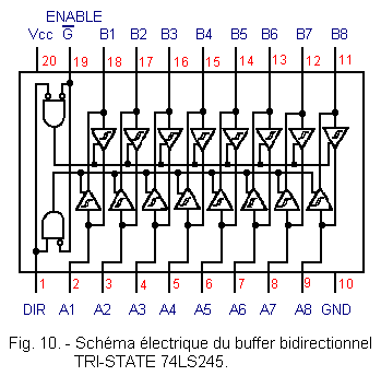
SECOND TEST : 74LS245 BUFFER TEST
In this second phase of the experiment, you will test the 74LS245 integrated circuit ; it is an eight-way transceiver whose electrical diagram is shown in Figure 10.
This bidirectional buffer is basically identical to that seen previously : the only difference lies in the number of channels (eight instead of four) and in the controls.
The control inputs AB
and GBA have been combined into a single one called DIR (executive abbreviation) ; there is in addition a control input called ENABLE
(enable = validation) which, when it is high, puts the buffer in the high impedance state and isolates it from the rest of the circuit.
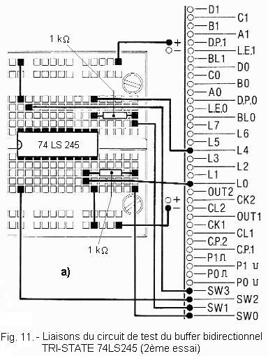
3. 3. - REALIZATION OF THE CIRCUIT
a) Remove from the matrix all the components and connections relating to the previous experiment.
b) Insert the integrated circuit 74LS245 and the two resistances of 1 kΩ on the matrix and carry out the connections indicated Figure 11-a.
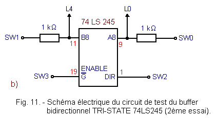
The diagram of the assembly carried out is given Figure 11-b. The 74LS245 buffer test method is the same as that adopted for the 74LS243 buffer.
c) Put the four switches on position 0.
d) Switch on the digilab and switch SW0 and SW1 to position 1, observing the effects on the LEDs L0 and L4 ; you will notice that if SW2 is on 0 (DIR input at low level), terminal B8 works as input and terminal A8 as output. If SW2 is in position 1 (DIR input at high level), the opposite occurs : B8 functions as an output and A8 as an input.
e) Observe now the effects produced by SW3 if one puts it on position 1 : by switching SW1 and SW0, you note that the buffer is isolated, that is to say that L0 and L4 turn on and off independently of each other.
This means that the control input
validates the passage of signals through the buffer only when it is at the low level and prohibits this passage when it is at the high level.
f) At this stage, check the operation of the other buffers contained in the integrated circuit by proceeding in the same way as for the first.
g) The circuit test finished, switch off the digilab.
3. 4. - CONCLUSION
This experiment allowed you to examine two bidirectional buffers, one with four channels of the type 74LS243 and the other with eight channels of the type 74LS245.
The two buffers operate identically and are differentiated only by the control inputs.
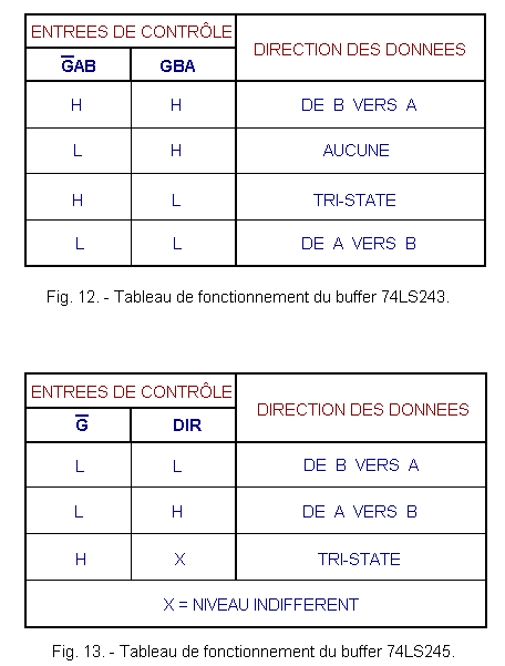
Figure 12 shows the operating table for 74LS243 while Figure 13 shows that for 74LS245.
These two tables summarize what you saw during the experiment.


 Footer
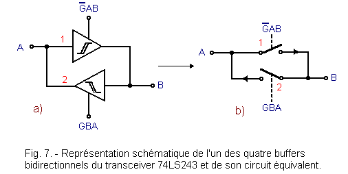
 Click here for the next lesson or in the summary provided.
 Top of page
 Next Page