In this practice, you will perform an interesting functional check of the Z80 microprocessor and continue the examination of the auxiliary circuits that surround it.
On the Digilab or BREAD BOARD (Plate used for experimental setups), you will check the operation of the RESTART circuit, the buffer circuits (BUFFERS) and the microprocessor address bus.
1. - PREPARATION OF THE MATERIAL
The components that will be used to perform the experiments planned in this practice are the following :
1 microprocessor Z80 or its equivalent
1 integrated circuit 74LS08,
1 integrated circuit 74LS14,
2 integrated circuits 74LS74,
1 integrated circuit 74LS86,
1 integrated circuit 74LS164,
1 integrated circuit 74LS243,
1 integrated circuit 74LS257,
1 integrated circuit 74LS245,
1 transistor BC559B,
1 resistance of 22 W
1 / 4 W - tolerance ± 5 %,
1 resistance of 220 W
1 / 4 W - tolerance ± 5 %,
1 resistance of 270 W
1 / 4 W - tolerance ± 5 %,
12 resistances of 1 kW
1 / 4 W - tolerance ± 5 %,
1 resistance of 1,2 kW
1 / 4 W - tolerance ± 5 %,
1 capacitor of 33 pF,
1 capacitor of 1 000 pF or 1 nF.
2. - FIRST EXPERIENCE : RESTART CIRCUIT OPERATION TEST
In the previous practice, you examined the reset circuit (RESET) which initializes the microprocessor when it is powered up or during its operation at any desired time.
The RESET command allows, among other things, to reset the address that the microprocessor provides to the address bus.
We know that data and instructions are stored in computer memory and that the microprocessor can take them as it needs them.
For this, the microprocessor must indicate to the memory the position at which the information it desires is located, that is to say, it must provide the address.
The latter is formed of sixteen bits and the microprocessor therefore has sixteen address outputs, one for each bit ; these microprocessor outputs are connected to the address bus on which all the address lines of the memories and, possibly, other input / output circuits are connected.
With sixteen bits, you can perform all combinations between 00 ... 00 and 11 ... 11, that is to say, in hexadecimal, between 0000 and FFFF. Each of these combinations corresponds to a specific address ; we therefore have 216 = 65 536 different addresses for a capacity of 64 kilobytes.
When the RESET input is activated, the microprocessor is forced to address zero, which means that, on the address bus, sixteen low levels appear.
Thus, the microprocessor begins execution of the program at address zero.
If you want the program to start at a no zero address, you must use a RESTART circuit (redémarrage), the operation of which we will now experience.
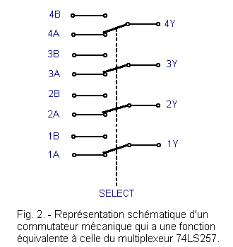
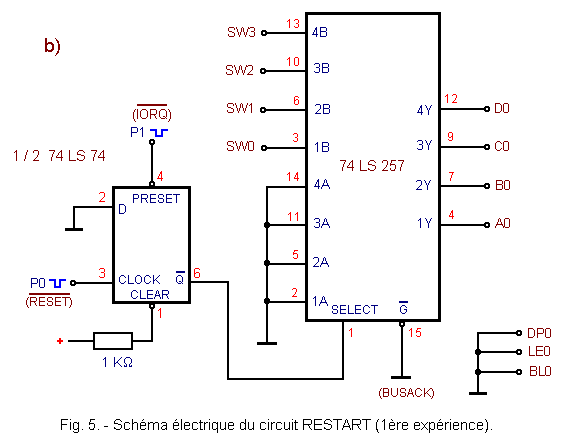
In this experiment, the integrated circuit 74LS257 is used which is a quadruple two-way multiplexer with three-state outputs. This circuit has eight main inputs, divided into two groups of four, and four outputs.
Depending on the state of the SELECT command input, the outputs are connected to one or the other group of inputs.
In practice, this circuit has a function analogous to that of a four-way, two-position mechanical switch, like the one in Figure 2.
The SELECT command establishes the position of the common contacts of the four reversers which, by switching simultaneously, allow the transfer to the outputs of the signals present at the four inputs identified by the letter A or at the four inputs B.
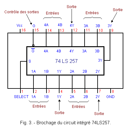
The pinout of the 74LS257 multiplexer is given in Figure 3.
The entry
is used to control the exits : when it is at the low level, the circuit behaves as we have just described it ; on the other hand, when it is at the high level, the outputs are put in the high impedance state (TRI-STATE). It is as if the inverters of Figure 2 were between two positions.
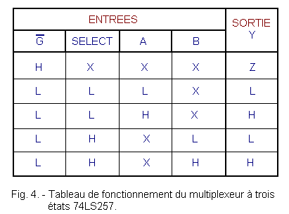
The operation of the multiplexer is summarized in the table in Figure 4 ; remember that the letter X means "indifferent" and indicates that the level present at the input has no influence on the output levels, while the letter Z indicates the state "high impedance".
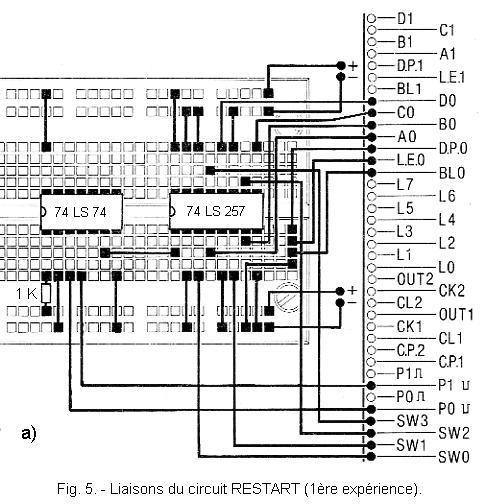
a) Remove from the matrix all the components and connections relating to the previous experiment.
b) Insert on the matrix the integrated circuits 74LS74 (double synchronous rocker type D) and 74LS257 (quadruple multiplexer two ways) and a resistance of 1 kΩ in the positions indicated Figure 5-a.
c) Make the connections shown in this same figure.
The electric diagram of the circuit carried out is represented Figure 5-b. By referring to it, carry out a careful visual inspection of the assembly.
NOTE:
It is interesting to check the connections relating to each pin of the integrated circuits.
We therefore first check all the connections relating to pin 1, then those of pin 2, then those of pin 3 and so on, in order, all the remaining pins of the integrated circuit.
In the same way, the connections of the second integrated circuit are checked. Finally, the connections relating to the displays and to the power supply of the integrated circuits are checked, these being usually omitted in the electrical diagrams.
2. 2. - FUNCTIONAL TEST OF THE RESTART CIRCUIT
a) Place the switches SW0, SW1, SW2 and SW3 in position 1.
b) Switch on the digilab.
c) Press P1.
d) Observe DIS0 : it indicates the number 0.
Indeed, by pressing on P1, one applies a negative impulse on the PRESET entry of the rocker and its exit
thus passes to the low level.
Consequently, the SELECT input of the multiplexer is also brought to the low level and selects inputs A. The outputs Y are therefore connected to these inputs : at output 1Y, we find the level present at input 1A, at output 2Y we find the level present at entry 2A and so on.
The four outputs of the multiplexer are all low and the display shows the number 0.
We will now perform the RESTART procedure.
e)
Press P0 and release : in this way, we simulate a negative pulse similar to that produced by the reset circuit (RESET).
At the time when P0 is released, a positive edge is applied to the clock input, which brings the flip-flop to the low level. The output
is brought to the high level and the multiplexer controlled by the SELECT input connects the outputs to the inputs B. The state of these is imposed by the position of the switches SW0, SW1, SW2 and SW3.
f) Observe the DIS0 display : it indicates the letter F.
g) Press P1 : the display DIS0 again indicates 0.
h) Switch off the digilab.
2. 3. - CONCLUSION
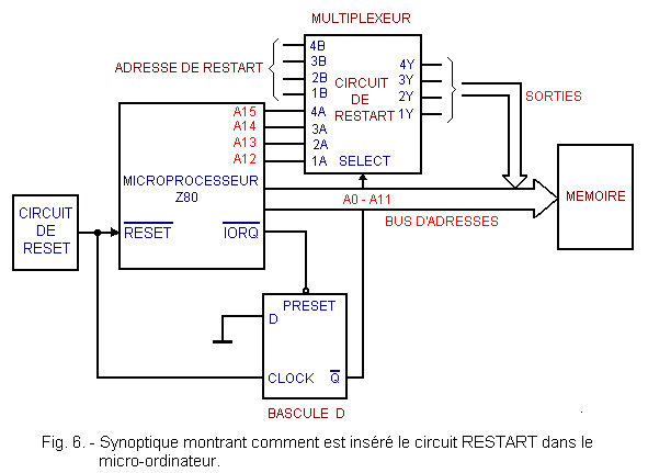
The operation of the RESTART circuit is simple. Observe Figure 6 which shows the circuit inserted on certain Computers System : you notice that the inputs A of the multiplexer are connected to the outputs of address A12, A13, A14 and A15 of the microprocessor Z80 ; in our experience, these outputs have been replaced by an earth connection (0 V = level L).
Entrances B are pre-positioned according to the address to which you want to depart ; in the experiment carried out, the address bits A12 to A15 are simulated by the switches.
When a pulse is applied to the input of the RESET circuit, all the address outputs of the microprocessor are brought to the low level, the flip-flop D switches and the multiplexer links its outputs with the inputs B.
Thus, the microprocessor begins the execution of the program at the selected address.
The address bits between A0 and A11 do not change because they are connected directly to the address bus. The four bits A12, A13, A14 and A15 take the predisposed value on the inputs B.
When the microprocessor has read the data which is at the memory address thus selected, it generates a pulse at the output
which brings back the rocker in the initial conditions. It is then ready for a new cycle of RESTART. The multiplexer again links the outputs to addresses A12 to A15.
To simplify, the
and
pulses have been replaced by those obtained manually by pushbuttons P0 and P1.
In addition, not having the microprocessor outputs available to us, the A inputs were connected to ground.
This corresponds entirely to the actual operation of the circuit because, when the reset key is pressed, all the address outputs of the microprocessor are automatically brought to the low level.


 Operation of the RESTART circuit
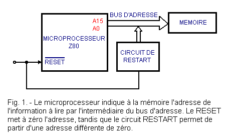
 Click here for the next lesson or in the summary provided.
 Top of page
 Next Page