6. - FOURTH EXPERIENCE : CHECKING THE WAITING CIRCUIT (WAIT)
The microprocessor may have to receive data from memories or circuits slower than itself and therefore may have to wait for the data to be available.
In this hypothesis, we have adapted an input circuit called WAIT, which in English means precisely to wait.
In certain phases of its work, the microprocessor observes the voltage level at the WAIT input and, if the level is low, it waits until it becomes high.
In this experiment, you will examine a circuit that, on command, produces a wait request (WAIT) for the duration of a clock period.
6. 1. - REALIZATION OF THE CIRCUIT
a) Remove the connections and connections used during the previous experiment.
b) Insert the integrated circuit 74LS125 (quadruple buffer TRI-STATE), the two circuits 74LS74 (each containing two rockers of type D) and the resistance of 1 kΩ in the position indicated in the Figure 16-a.
c) Make the connections indicated on the Figure 16-a.
d) Place the clock generator 1 on the 1 Hz position.
The electric diagram of the circuit which you carried out is represented in the Figure 16-b. In this diagram, you can observe the presence of a component that you do not yet know : it is the integrated circuit 74LS125 which contains four non-inverting buffers whose outputs can be brought to the high impedance state (TRI-STATE) by means of the control input.
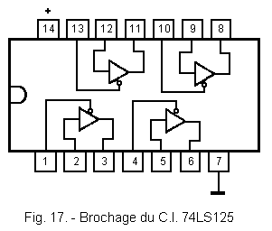
We will examine below the functioning of this integrated circuit ; the pinout diagram is shown in Figure 17.
6. 2. - OPERATION TEST
a) Switch on the digilab : you will see that the L0 LED turns on and off once per second since it is controlled by the CP1 oscillator, while the L4 LED is on.
b) Observing the LED L4, press the P0 key for at least one second : you see that L4 goes out at the very moment when L0 lights up and that it stays off for one second, which corresponds to the period of the clock and indicates that the level of the output voltage of the circuit (point A of the Figure 16-b) fell to the low level.
You have therefore experienced the operation of the waiting circuit. To better know the details, we will now examine the two parts separately : the one made up of the three rockers and the one made of the 74LS125 buffer.
The circuit of the first part is widely used in many applications and has the property of generating a long pulse, of duration equal to the clock period.
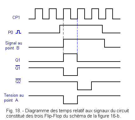
The diagrams of times of the Figure 18 represent the signals relating to the circuit made up of the three rockers of the diagram of the Figure 16-b.
The purpose of the first flip-flop is to synchronize the signal from the P0 key so that its rising and falling edges coincide with the rising edges of the clock signal.
Indeed, the action of pressing P0 is independent of the internal logic and can occur at any time.
In some computers, the corresponding signal will already be synchronized, so the first switch will not be necessary. As soon as the signal at B goes high, the second flip-flop intervenes and Q1 goes high.
At the next pulse from the clock CP1, the third flip-flop is validated since its input D is at the high level. Consequently, the exit 2
will go down to the low level and, by the entry CLEAR, one will reset to zero the second rocker, by instantaneously putting back its exit Q1 to the low level.
Let us now examine the second part of the circuit of the Figure 16-b, constituted by the buffer 74LS125.
The buffer is of the TRI-STATE type, its output can therefore follow the level of the input signal or be in the air, high impedance, depending on the level applied to the control input C.
The table in Figure 19 summarizes the operation of the buffer. If C is low, the output level is also low ; on the other hand, if C is at the high level, the output is high impedance.
Fig. 19. - Buffer 74LS125 operating table.
Entry
Order C
Output
L
L
L
H
L
H
X
H
High impedance
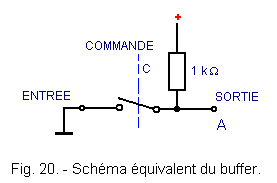
In practice, we can say that the buffer behaves like a switch controlled by C and wired as shown in Figure 20.
When 1,
therefore C also, is at the high level, the switch is open and the output A is at the level of the positive tension via the resistance of 1 kΩ. If on the contrary, 1
is at low level, the switch is closed, the output is at low level and provides a wait signal to the microprocessor.
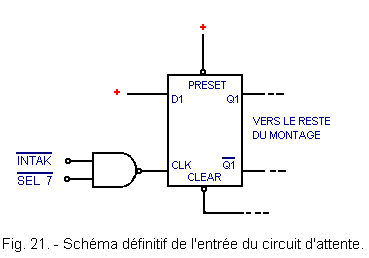
Last observation : the circuit examined is a little different from that which you will find on Computers. The first flip-flop in the final version includes, at its entrance, a NAND gate connected as shown in Figure 21.
The two signals arriving at the NAND gate come from other parts of the microcomputer.
is delivered by the PROM of decoding of the memory, seen in the third experiment, which is programmed so as to carry out a waiting cycle for the slow memories.
In the tested circuit, the first flip-flop synchronizes the signal from point B, at the clock input of the second flip-flop, with the clock that controls the third flip-flop.
Indeed, the signal from the P0 key is asynchronous, that is to say that this button can be pressed at any time.
On the contrary, the signals
and
are synchronous and therefore do not require any synchronization.
This holding circuit, the subject of our test, is necessary when the microprocessor is working at high speed, and it is only necessary when a 4 MHz clock signal is used.


 Footer
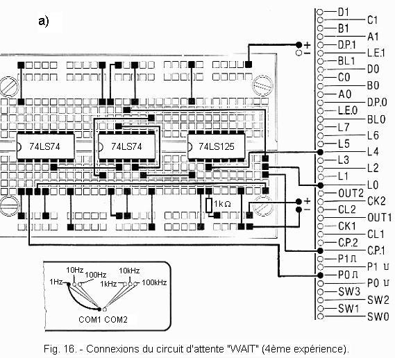
 Click here for the next lesson or in the summary provided.
 Top of page
 Next Page