Functional Test of the Z80 Microprocessor by the Signature Method :
4. - THIRD EXPERIMENT : FUNCTIONAL TEST OF THE Z80 MICROPROCESSOR BY THE SIGNATURE ANALYSIS OR "SIGNATURE ANALYSIS" METHOD
In this experiment, you will start by testing the Z80 microprocessor ; for this purpose, you will use a very interesting method called "signature analysis".
This method is generally applied to test complex digital equipment ; it is based on the fact that certain signals are periodic, that is to say repeat cyclically and therefore have a typical "signature". During the experiment, you will better understand the meaning of "signature".
The devices for "signature analysis" are quite complicated and expensive. In this experiment, we will adopt a simplified but effective control circuit.
THE Z80 MICROPROCESSOR
The Z80 microprocessor is in the form of a 40 pins integrated circuit, inside which are found almost all the elements necessary for a microcomputer, except the memory which must be external.
To this must be added auxiliary circuits, some of which have already been examined, such as the clock generator, the reset circuit, etc. ...
For the moment, we will not approach the internal constitution of the Z80, it will be approached in the theoretical lessons in the form of a synoptic diagram, but we will check if the copy works regularly.
Let's take a look at the pinouts first and review some input and output signals.
By observing Figure 14, you notice that, on the right side, are grouped all the pins corresponding to the outputs.
The pins marked with D0, D1, D2, D3, D4, D5, D6 and D7 are special cases because they can be inputs or outputs.
Indeed, one can find on these pins either the data that the microprocessor can receive from the outside (for example memories), or that which it transmits.
In this experiment, we will use many inputs and outputs including those noted from A0 to A15.
These outputs are used to supply the address signals by which the microprocessor indicates the position of the memory box in which it wishes to read or write information. This, consisting of 8 bits, travels on the lines from D0 to D7.
Pin 6, marked with the symbol f,
is the input to which the clock signal must be applied.
Among the other inputs, you already know the entry
(pin 24) which must be connected to the WAIT circuit (standby) and the entry
(reset to zero, pin 26) which must likewise be connected to the RESET circuit.
The remaining inputs and outputs have specific functions which will be examined later and which also concern memory management.
NOP INSTRUCTION
To fully understand the mechanism of the experiment, it is necessary to know certain peculiarities of the operation of the Z80.
First of all, it should be specified that in addition to the data to be processed, it reaches the inputs D0 to D7 with instructions indicating to the microprocessor what to do.
Among the many instructions of the Z80, there is one, called NOP, which requires it to do no operation and go to the next instruction ; in fact, the acronym NOP is the abbreviation for no operation.
The Z80 recognizes the NOP instruction if all the inputs D0 to D7 are low.
Let us now see what is the way of operating the microprocessor.
The start of operations is given by a reset command. Immediately afterwards, the Z80 presents on the outputs from A0 to A15 the address 00 ... 00 (binary), that is to say 0000 (in hexadecimal code) and at the same time it presents, on the inputs data, the instruction stored in memory at the address 0000 (hexadecimal).
This instruction is executed by the microprocessor which then increments the address which therefore goes to 0001 ; the instruction contained at this address is read and then executed.
The microprocessor then goes to the next instruction at address 0002 and executes it. The instructions are therefore read and executed one after the other.
The sequence of instructions constitutes the program.
Practically, the process is a little more complex since the instructions can occupy more than one memory address and the microprocessor can jump from one part to another of the memory according to the instructions it receives.
However, for our experience, the description of the operation that we have just done is sufficient. In fact, an NOP instruction occupies a single memory address and does not cause the microprocessor to leave the normal operating sequence.
Throughout the experiment, the microprocessor will be made to execute a sequence of NOP instructions. In this way, it can only read the instruction and increment the address in the following sequence :
RESET
or remise à zéro (must be done at the start of operations)
ADDRESS
0000 provided by the outputs from A0 to A15
The Z80
reads NOP (ordered to take no action and go to the following address)
ADDRESS 0001
The Z80 reads NOP
ADDRESS 0002
The Z80 reads NOP
ADDRESS 0003
The Z80 reads NOP
ADDRESS 0004
The Z80 reads NOP
We continue by always increasing by one unit until :
n - ADDRESS FFFF
n + 1 - The Z80 reads NOP
n + 2 - ADDRESS 0000
n + 3 - The Z80 reads NOP, and so on.
We can see that the microprocessor generates all the possible addresses from 0000 to FFFF (in hexadecimal) and then start again from the beginning.
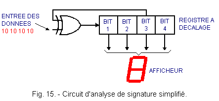
Signature analysis is a technique, introduced by the Hewlett Packard company, which identifies possible errors in a data sequence.
This sequence is transformed into a number of several digits, four in general, but limited to two in our experience. This number represents the signature of the sequence. It is characteristic of this sequence, at a given point in the circuit. We save it, then we check the correct functioning of the circuit by reading again the number that the signature represents : each difference with that recorded previously indicates an irregularity of operation.
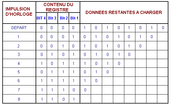
An example will help you better understand. Suppose that we have the sequence of bits 10 10 10 10 and that we want to obtain the signature by the circuit of Figure 15 constituted by a shift register and an Exclusive OR gate.
The data is applied to one of the inputs of the Exclusive OR gate, while the other input receives the bits of the third stage of the register. It is assumed that the register is set to zero at the start, that is to say that it contains four zeros.
We therefore introduce the data by eight clock pulses, starting by loading the first bit on the left. As the data enters, the content of the register changes and consequently, the content of the stage relating to bit 3 too. The data present in this stage being applied to one of the two entries of the Exclusive OR, also influences the data which enter the register.
The resulting sequence is as follows :
At the end of the operation, there is therefore in the register the number 1101 which will be displayed on the display by the hexadecimal digit D. This digit constitutes the signature of the sequence examined.
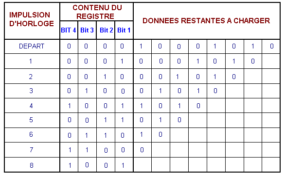
Now let's see what happens if the sequence contains an error because the third bit is for example 0 instead of 1. In this case, the loading of the register is done as follows :
This time, the register contains the number 1001 which will be displayed on the display by the number 9. The signature is false, the error on the third bit has been detected.
Note that the same result could be obtained without an Exclusive OR gate by using an eight bits shift register for any number of data to be examined.
However, this solution becomes impractical if the sequence is very long ; indeed, it sometimes includes hundreds of data.
For signature analysis, on the other hand, a reduced size register is sufficient. An error, even if it is at the beginning of the sequence, does not go unnoticed ; it is transmitted as the data enters and influences the end result.
In the following experiment, an eight bits shift register is used so as to obtain a two digits signature.
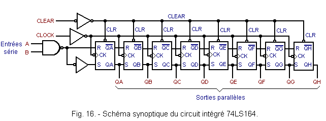
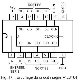
The Figure 16 shows the block diagram of the integrated register used, the 74LS164, while Figure 17 gives the pinout.
It is a shift register of the series-parallel type with eight stages, each of them being constituted by a rocker.
The data can be applied to two inputs marked A and B ; in the experiment, only input A is used (pin 1).
The shift takes place on the rising edge of the clock signal. The CLEAR entry which resets the register to zero, is active on a low level and is asynchronous ; in other words, as soon as a low level is applied to this input, the register is reset to zero without having to wait for a clock pulse, as synchronous operation would require.


 The Signature Analysis
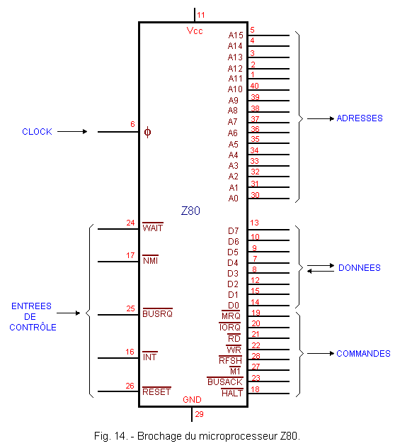
 Click here for the next lesson or in the summary provided.
 Top of page
 Next Page