In this theory, we will examine the logical family of MOS transistors. Other logical families will be mentioned. Finally, we will discuss the manufacture of integrated circuits.
1. - LOGIC FUNCTIONS WITH FIELD EFFECT TRANSISTORS
Junction field effect transistors are not used to materialize logic functions.
On the other hand, the insulated gate field effect transistors, TEC-MOS, are very used. They allowed the crossing of an additional step in the field of integration of functions.
This is due, in part, to the relative ease with which they can be realized with respect to the bipolar transistor and their low consumption (thus low dissipation resulting in low temperature rise per mm2 of integrated circuit).
They can replace ohmic resistances, which is very important in terms of integration, because they occupy a lot of space and especially as their values are important.
We know that there are N-channel, P-channel, enrichment or depletion MOS (also called depletion or necking).
If one wants to maintain a certain compatibility between TTL and MOS technology, it is imperative to keep the same polarity for the power supply, which can be implemented easily with the N channel. On the other hand, the enrichment mode is simpler to achieve.
It will therefore be a question first of MOS channel N enrichment. Then, we will see that there is another way of proceeding with what the specialists call the COS - MOS or C - MOS (complementary symmetry - MOS) technology which uses the N channel and the P channel
1. 1. - THE BASIC DEVICE IN N-MOS TECHNOLOGY
Figure 1-a shows the basic device. It is an inverter circuit as evidenced by its truth table.
In the absence of voltage Ve
on its input ; either Ve = low level
or state 0, the transistor is off and
Vs (output voltage) is equal to + VDD
either the high level or state 1.
In the opposite case, Ve
= + VDD high level or state 1.
The transistor is conductive and Vs
is low or state 0.
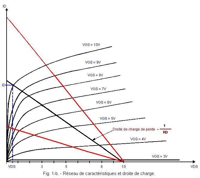
Figure 1-b shows its characteristic network and its slope load line -
(1 / Rd) (Rd = drain resistance).
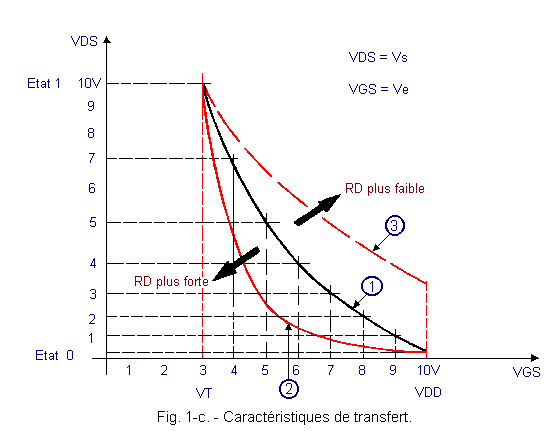
Figure 1-c illustrates the transfer characteristic of this arrangement. The voltage VDS represents the output voltage Vs. The voltage VGS is the input voltage Ve.
When an input voltage is applied, the output voltage remains stable and high until the voltage VT, or threshold voltage, for which the transistor starts to drive is reached, and then continues to increase the input voltage, VS decreases according to the curve
to the low level or state 0.
One realizes that the more the resistance RD is strong, the more one reaches quickly the low level (curve ).
On the other hand, if RD is too weak, the low level is obtained for an input voltage Ve greater than the voltage VDDVDD (curve ).
It is therefore rather towards a large RD that we will orient ourselves, but we know that the realization, on an integrated circuit, of a resistance of high value poses a serious problem.
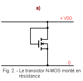
Figure 2-a provides a solution to this pitfall.
If the gate is connected to the drain of an enriched N-MOS transistor (N for N-channel) and ID is recorded as a function of VDS, the curve of Figure 2-b is obtained.
Practically, this one is a line which does not pass by the origin of the axes.
This line represents approximately the characteristic curve of a resistance.
The offset on the axis of the VDS voltages can be likened to a voltage in series with this resistance, shown schematically in Figure 2.-c.
The transistor, mounted in this way, therefore behaves like a resistor in series with a voltage generator VT.
Up to VDS = VT, the currentID
is extremely low, beyond that, it grows almost linearly with VDS
(see Figure 2-b).
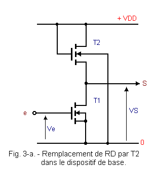
We come to Figure 3-a, where we replaced RD by T2.
The T2 substrate is connected to the reference potential 0 because it must always be at the most negative potential of the assembly.
In Figure 3-b, we find the VDS function ID network of transistor T1 and the load line whose slope is the inverse of the resistance obtained with T2. By construction, we make sure that this resistance is strong enough to reduce as much as possible the transition time between the two states of T1.
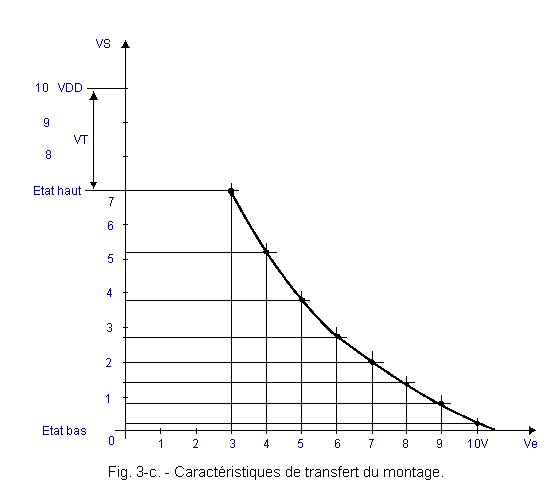
Figure 3-c shows the transfer characteristic of this arrangement. It should be noted that the output voltage at the high state is no longer equal to + VDD
but to :
VS = + VDD - VT
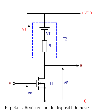
Indeed, Figure 3-d, we find :
VDD = VT + VDS (T1)
VDS (T1) = VDD - VT
By neglecting the voltage obtained by the product of R
and the leakage current of T1 (this current is extremely weak).
The
Figure 3-a is the final version of the basic device, the N-MOS transistor-enriched inverter.
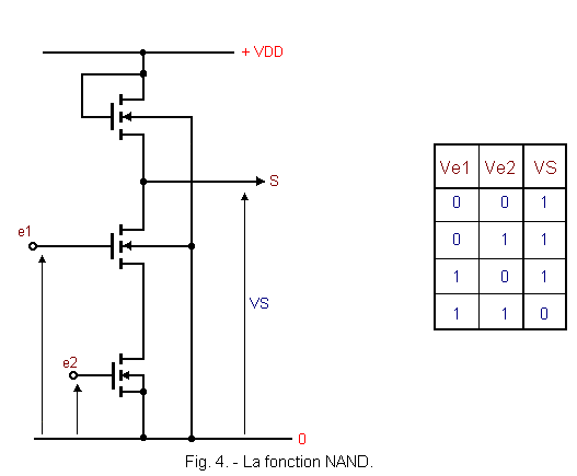
Figure 4 shows the NAND in N-MOS technology and its truth table.
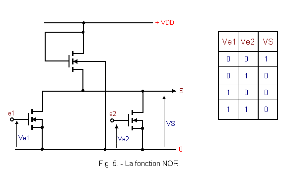
1. 1. 2. - NOR FUNCTION
It is shown schematically in Figure 5 with the table of truth that relates to it.
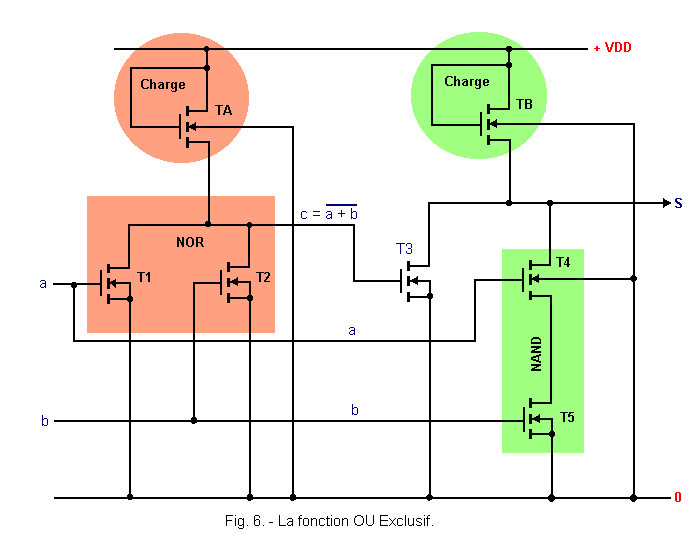
1. 1. 3. - FUNCTION OR EXCLUSIVE
Figure 6 shows the device used for the construction of an Exclusive OR.
A NOR function is used around T1 and T2 and therefore the load is TA (identical to NOR in Figure 5), a NAND function consisting of T4 and T5 and whose load is TB (identical to the NAND of Figure 4).
The transistor T3 is mounted in an inverter. At its output, the signal is a + b.
The output of this transistor is connected to the output of the NAND operator.
These two outputs therefore perform the AND function "wired".
Indeed, if one of the outputs a + b or goes to the state 0, the output S goes to state 0.
So S = (a + b) .
Let's apply the property of the distributivity of the logical product with respect to the logical sum :
S = a .
+ b .
Let us replace by +
(De Morgan's theorem).
S = a (
+ )
+ b (
+ )
= a
+ a
+ b
+ b
= a
+ b
(since a
= b
= 0) =
Thus, the assembly of Figure 6 which realizes the Exclusive OR function, uses in all and for all only seven MOS transistors. In TTL technology, this function would have required the use of four NAND gates, see sixteen transistors. This leads us to say that MOS technology is a relatively low cost (the cheapest of all).
Consumption is lower than for TTL, but remains high enough to limit the level of integration.
On the other hand, the speed (that is, the maximum operating frequency) of these devices is quite low.
Noise immunity is better than with TTL.
Since you always have to evolve, the next step is drawn. Why not use complementary MOS transistors ?
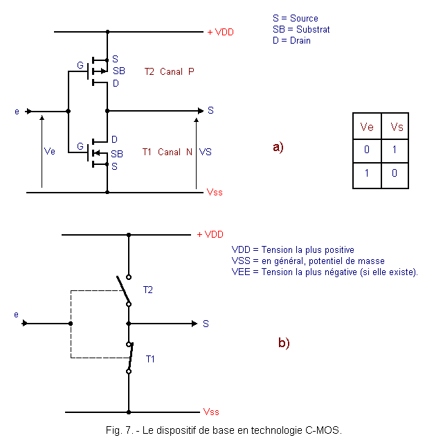
Figure 7-a corresponds to the basic device. It is a transistor T2 channel P connected in series with a transistor T1 channel N. The two grids are united and form the single control.
The source and the T2 substrate (P channel) are connected to the + VDD while the corresponding electrodes of T1 (N channel) are connected to the reference potential (which in this case is called Vss).
Operation is illustrated in Figure 7-b. When the input voltage Ve is high (state 1), the transistor T1 is conducting while T2 is off.
Output S is low (state 0). The consumption of the assembly in this state is practically zero.
When the input is brought low (state 0), the transistor T1 is blocked and T2 becomes conductive (the voltage VGS of T2 being negative).
Output S is high (state 1). Consumption in this new state is still practically nil.
Once again, the basic device is an inverter mount.
If the consumption, in the two static states of the montage, is zero, it is not the same at the moment of the transition which separates these states. For a short time, the two transistors are simultaneously conducting thus creating a current draw. In complex logic systems, if the input often changes state, the current draw is manifested much more often and operation, at a high frequency, corresponds to an almost permanent consumption so important.
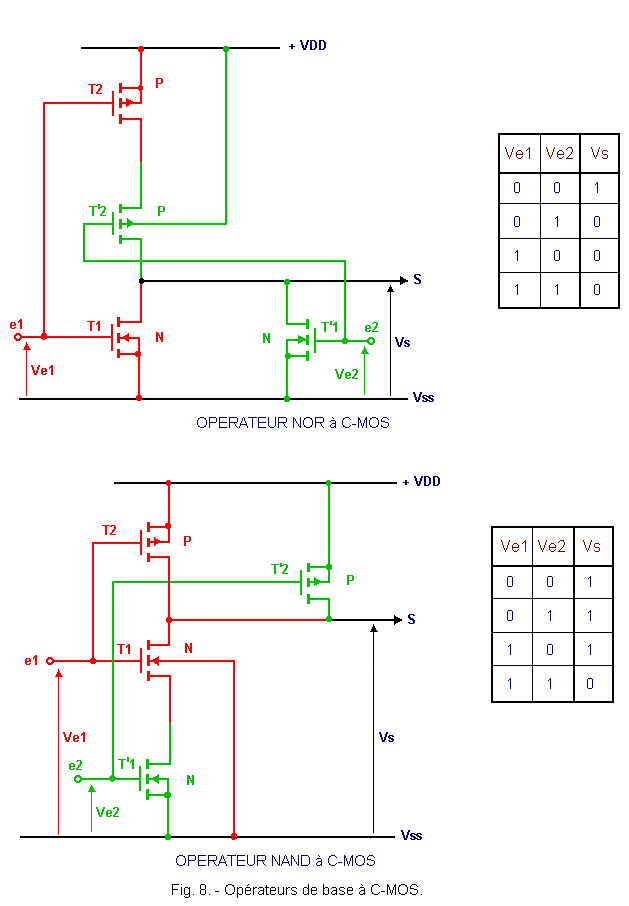
1. 3. - BASIC OPERATORS IN C-MOS
They are shown in Figure 8, with their truth tables.
These are the circuits performing the NOR function and the NAND function.
Each pair of transistors is identified by T1 and
T2
so that the analogy is easier for you compared to the basic setup of figure 7-a.
This technology, despite its higher manufacturing cost than the N-MOS, is more widespread than the latter.
The speed of operation is lower than for the TTL, which is much more expensive, however, it tends to settle very strongly in relation to it.
Its immunity to noise, much better, designates it for industrial assemblies in disturbed environment.
The number of built-in functions is now comparable to that of the TTL which was, up to now, clearly in the lead.
Finally, a new series, made under the name 74 C ..., is the exact replica, as regards the case, the pinning and the voltages of the TTL series, it is therefore directly interchangeable with the latter.
In industrial systems, it seems that currently, these two technologies dominate over others.
Another advantage of the C-MOS is its supply voltage range : from 3 volts to 18 volts.
Its propagation time is a function of the supply voltage and it decreases with the increase of the latter. To compare with the TTL, these times will be given with a power supply of 5 volts.
tPHL
= 35 ns
tPLH
= 100 ns
The static noise immunity, for the same supply voltage, is 1.5 volts minimum.
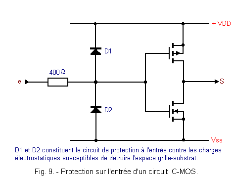
The disadvantage, compared to bipolar technologies, is its fragility with respect to the static charges, due to the high impedance of the inputs.
Protection circuits, made with diodes, are placed on all the inputs between these and the two power poles (Figure 9 shows the protection circuit).
Despite these measures, it is necessary, when handling, to take a number of precautions (low-voltage soldering iron, avoid clothing made of synthetic material and carpets or rugs).
It is even advisable to connect the wrists of the manipulators, with the help of bracelets, to a good grounding.


 NAND, NOR, OR Exclusive Functions in N-MOS
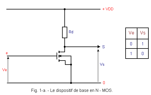
.gif)
.gif)
).gif)
 Click here for the next lesson or in the summary provided for this purpose.
 Top of page
 Next Page