The monolithic qualifier means a single block, that is to say that the passive and active components are all made during the same operations on the same substrate.
These circuits are based on two technologies, one with bipolar transistors, the other with MOS transistors.
Then we find two destinations, one for digital circuits, the other for linear or analog circuits.
A third category allows the classification of these circuits is the level of integration or, in other words, the density of components or operators per unit area (say per square millimeter).
This classification is not very strict yet and sometimes depends on the builders. It allows, however, for the observer, to note the tremendous evolution in this field.
There are three levels that are :
The
S.S.I.
(Short
Integration) or integration on a small scale, which corresponds to the first circuits and whose integration covered a dozen operators or logic gates.
The M.S.I. (Medium
Scale Integration) or medium scale integration, for which the level can reach 100 logical gates.
The
L.S.I.
(Large
Scale Integration), integration on a large scale, which involves an integration of more than 100 logic gates.
We also speak of V.L.S.I.
and S.L.S.I. (Very
Large Scale Integration and Supra Large Scale Integration). It involves the integration of more than
10 000, or more than 50 000 transistors on the same chip. To situate a little better the problem, it is necessary to know that the microprocessors are in the L.S.I..
Figure 14 shows the different orientations that lead to the classification of a monolithic integrated circuit.
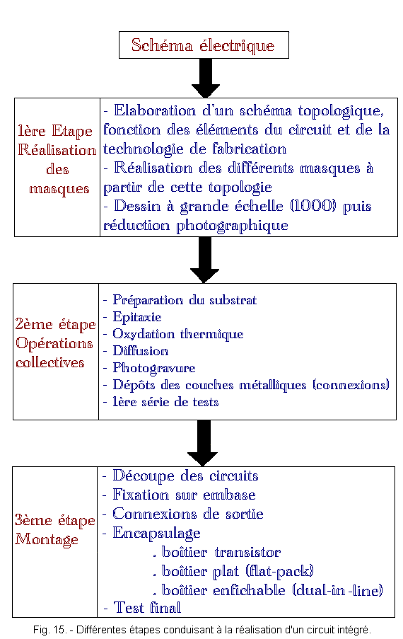
3. 4. 1. - MONOLITHIC INTEGRATED CIRCUITS IN BIPOLAR TECHNOLOGY
The realization of these circuits comprises three main stages which are :
the realization of the masks
collective operations
individualization and assembly of the circuit
From a function to be realized, digital circuit or analog circuit, an electrical diagram is elaborated.
From this diagram, we will draw the drawings corresponding to the different masks to be made.
The so-called collective operations that use the aforementioned masks and which apply to the PLANAR process are then carried out. There are others for the realization of circuits, but they derive more or less from it.
Finally, the circuits are cut and individualized and then mounted on a base with connections, encapsulated and tested.
Figure 15 summarizes the various steps of the realization of a bipolar integrated circuit in the form of a table.
The Planar process is also used in the realization of semiconductors (diodes, transistors).
The collective operations relating to this process, which are of a physico-chemical nature, deserve some comment.
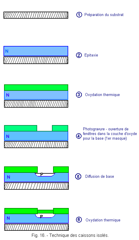
The preparation of the substrate consists of producing a silicon wafer which will serve as mechanical support and on which several hundred identical circuits will be implanted. These platelets have a diameter of the order of 5 to 10 centimeters and a thickness of 200 to 300 microns. Their surface condition must be as perfect as possible, which requires a polishing operation.
Epitaxy consists of depositing a semiconducting layer of extrinsic conductivity (due to doping) and of well-controlled thickness on the substrate of which these parameters are less important, since it is a mechanical support. The thickness of this epitaxial layer varies between 5 and 10 microns.
Thermal oxidation allows the creation of a silicon oxide layer (0.5 micron thick) on the epitaxial layer.
This coating allows greater precision in the next operation, diffusion.
Then, by photogravure, windows are made in this coating through which the various diffusions will be carried out. These will, therefore, be perfectly delimited.
This oxide layer can also be put in place to protect the junctions made in the epitaxial layer, in the final phase.
Dissemination, we have already discussed in the chapter devoted to semiconductor and extrinsic conduction.
It is to diffuse, locally, a body (or impurity) in the semiconductor crystal lattice, in order to obtain the conductivity of P or N type (according to the atomic structure of the scattered body).
Stacking these types of conduction allows the creation of junctions, so diodes or transistors.
Resistances are also performed according to this method, in places where it is planned to implement them, that is to say by opening windows in the oxide by photoetching and use of masks. The range of resistances ranges from about 20 to 20 000 Ω.
The capacitors can be realized in two ways, either by the capacitive effect of a reverse-biased junction (which has been discussed with respect to diodes with variable capacitance), or by interposition between two metallized zones of a dielectric material ( silicon oxide). We thus obtain a few hundred picofarads.
Photogravure is used at each new stage in order to make the windows in the protective oxide.
This is the same process as that described for thin films.
Vacuum metal deposition is used to place in areas not masked areas capable of making the connections or connections between the elements and on which will be fixed the son of outputs. The thickness of this deposit is about 0.8 micron.
Here again, it is the same process as that used for thin films.
All of these different phases constitute the collective operations.
They can have up to eight different masks, each followed by one or more of the above phases.
These operations are performed on 1 000 to 10 000 circuits at the same time.
The last step is to cut the silicon wafers (used as support) on which have just been practiced collective operations in as many integrated circuits (from 100 to 1 000 circuits).
We thus obtain what we call chips. These are then fixed on the base of the housing, after which the connections are made between the circuit and the output pins of the base.
Then comes the encapsulation. Different boxes are proposed, depending on the dimensions of the circuit and especially depending on the number of outputs.
The integration is becoming larger, the outputs are more numerous, therefore, the housing is becoming larger.
These connection and encapsulation operations are performed on each circuit, they are therefore greatly involved in the cost, so much so that packaging is more expensive than the chip itself.
We will try to reduce the number of outputs per circuit, by assigning them different functions. This is the so-called multiplexing technique which consists, for example, of using four terminals indifferently as inputs or outputs. A fifth pin sends a binary logic signal (presence or absence of voltage) that controls the external peripheral circuits, indicating when the four pins are to be used as outputs or inputs.
The three-state logic is applied to the peripheral circuits. It allows to temporarily disconnect a number of these when the signals present do not concern them.
All cases are subject to very strict standards both in terms of size and technology.
For less complex circuits, transistors boxes with more outputs (6 or 8) are used.
For larger circuits, suitable boxes have been developed. These are, on the one hand, flat boxes (or flat-pack) that is connected to the printed circuit by micro-welds. They are generally intended for aerospace or military techniques, and secondly plug-in boxes (or dual in line) more specifically designed for industry. Outputs can be 64.
These two types of cases are made of ceramic for special applications (they are very expensive) or plastic.
In the following technology, you will find a collection of different housings used in electronics.
Before finishing with the monolithic circuits concerning the bipolar technology, it is necessary to speak of the isolated caissons.
Figure 16 shows the different stages of the realization of a transistor (this is a N.P.N.). It is assumed that it is part of an integrated circuit and that many other transistors (either N.P.N. or P.N.P) are arranged around.
It is obvious that we will be forced to build dielectric barriers delimiting each of these transistors to isolate them from each other.
These barriers are islands that are called isolated caissons.
There are several methods to achieve this isolation that are :
by junction
by EPIC process
by ISOPLANAR process.
Figure 17 shows ISOPLANAR isolation.
These insulated boxes are not only used for the active components but also for the passive components of the circuit (resistors, capacitors).
As an indication, the dimensions of the boxes are of the order of 100 x 100 microns.
They are also used in the manufacture of integrated circuits of MOS technology.
The design of the latter being somewhat different, we will devote the following chapter.
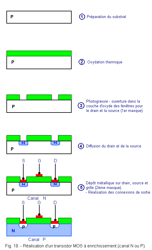
3. 4. 2. - INTEGRATED MONOLITHIC CIRCUITS IN MOS TECHNOLOGY
Figure 18 gives an overview of the embodiment of an enriched N-channel MOS transistor.
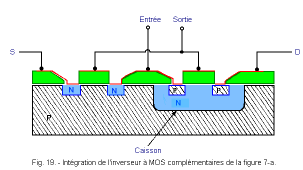
Figure 19 represents the integration of the basic inverter into C-MOS (complementary MOS).
We see a box appear. This is necessary because the substrate of a P-channel MOS transistor must be of conductivity N (see Figure 18) whereas that of an N-channel must be of conductivity P.
This inverter requires for its implementation less operations and its low consumption at rest allows a much greater integration than for the bipolar.
The isolated box, in this case, is of the order of 50 x 50 microns.
In addition, this technology does not involve the production of passive components such as resistors, since we know that a MOS transistor whose gate is connected to the drain behaves like a resistor.
Capacitors are produced according to the same principle as for producing the gates of these transistors, the dielectric being the silicon oxide layer.
We also take advantage of the grid-substrate parasitic capacitance (whose value can reach 2 to 5 pF), for the realization of the registers and dynamic memories which we will approach in a future theory.
This capability is, in large part, responsible for limiting the operating frequency of these devices.
So is it interesting to direct research towards a reduction of this capacity ?
In general, these parasitic effects are due to the fact that these zones are inside the substrate.
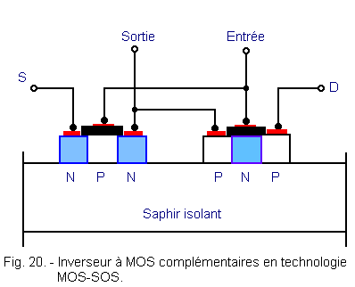
If an insulating substrate is used and on this support, the different layers of material are made in elevation, isolated islands are obtained, each of them representing an active or passive component well isolated from the others.
Figure 20 illustrates this process which takes the name of S.O.S. (Silicon On Sapphire : Silicium Sur Saphir).
The reduction of parasitic capacitances, leakage resistances, brings an increase in the operating speed in a ratio of the order of 5 to 10. The dynamic consumption is also reduced.
A new orientation is given to the MOS technology.
Two major factors guide the evolution of a technology :
the speed of operation
the consumption
If the operating frequency must be as high as possible, we will seek the lowest possible consumption, not for the sake of economy, but to be able to integrate more functions on the same support without reaching square millimeters, operating temperatures likely to damage the components or to bring drifts.
MOS-SOS technology is therefore an interesting achievement.
There are others, among them, the technologies Planox, Polyplanar, Isoplanar. One of the most important is the LOC MOS (Local Oxidation Complementary - MOS) whose list of functions performed in this technology becomes impressive.
We have just made a brief overview with regard to integrated circuits, this area is constantly evolving and our goal is not to describe all the technological achievements.
However, the technician must have some knowledge of these problems in order to make the best use of the circuits at his disposal or, when the time comes, to be able to choose one technology over another, depending on the destination of the device equipment.
This choice is generally made according to the following criteria :
Speed of operation
Consumption
Immunity to noise
Choice of the functions proposed by the manufacturer in the selected technology.
Cost price of the operators (in the case of serial construction).
The level of integration occurs in some cases, because you must know that the higher the integration, the better the reliability of the whole.
Reliability is defined as the probability that a device performs its function well under specified conditions of use and for a specified period of time.
This is one of the major advantages of integration, because many manipulations are removed during the production of a material using this technique and we avoid errors and defects.
All the parameters associated with the reliability are well defined, it is thus possible to quantify this value and the gain brought by this use is between 10 and 50, which is very important because it means that the devices thus designed will work without failure from 10 to 50 times longer than those made in the traditional way.
From the manufacturer's point of view, a technology has an outlet only if it brings an improvement in the cost price, performance and especially if there is reproducibility of these performances (little waste in manufacturing).
In the next technology, we will draw up an inventory of the logic circuits most frequently encountered in industrial assemblies. It will also be presented a lexicon of terms used in manufacturers catalogs as well as the different housings used for semiconductors and integrated circuits.


 Monolithic Integrated Circuits in Bipolar Technology
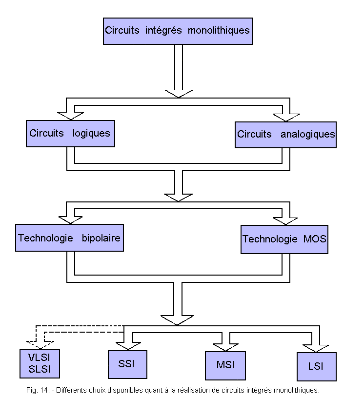
.gif)
.gif)
 Click here for the next lesson or in the summary provided for this purpose.
 Top of page
 Next Page