For TTL, Figure 28 clearly explains what is happening with the voltages and will allow you to introduce new parameters.
Immunity to noise.
A standard has been established (for each technology), it defines the voltage levels, for the input and the output of the operators, which symbolize the two logical states, this in the worst case (manufacturing limit tolerance, ambient temperature and maximum load).
When two operators are connected, the output of one on the input of the other, it is necessary to know the margin that remains for each of these states in order to evaluate the risk of an unwanted operation due to causes (industrial pests, fluctuating mass potential, ...) and take the necessary measures from the beginning to avoid any failure.
This is concretized in state 0, or low voltage level, by the difference between the maximum voltage that can take the output of the previous operator, for this state, and the maximum level that the input of the operator next will still consider a low level.
Beyond that, it will interpret it as a change of state and its output level will be modified accordingly.
In state 1, or high level of voltage, this is concretized by the difference between the minimum voltage that can take the output of the previous operator and the minimum level that the entry of the next one will interpret again as a high level.
Below, it will consider that it is a change of state and its output level will be modified accordingly.
These voltage differences characterize the noise margins, in the low state and in the high state. They determine what we call : noise immunity (called "noise", in this case, any parasitic signal foreign to the useful signal).
The output voltage at low VOL is 0.4 V.
The input voltage VIL considered as a low state is 0.8 V.
The difference between these two tensions gives us the zone marked by
which is the margin of noise in the low state.
The minimum output voltage at high VOH is 2,4
V.
The input voltage considered as a high state is 2
V.
The difference between these two tensions gives us the zone marked by
which is the margin of noise in the high state.
zone
represents the zone of amplification, in logic, it is a region which must be avoided.
Noise immunity or noise margin is very low in TTL (0.4 V in theory). In practice, this margin is considered to be 1 V assuming that there is little risk that a circuit having an output at the limit values will be connected to others whose input characteristics would also have values limits.
This noise immunity is important in the choice of a technology for a realization. We will see in a summary table that other technologies can have a better immunity to noise (or disturbing parasitic signals).
Another important parameter in the operator assembly is the fanout (or fan-out = output fan) or pyramid factor.
This is the number of circuits that can be connected to the output without significantly altering the circuit parameters.
The output with totem-pole assembly is performed for this purpose.
The normalized input current in the high state, IIH is + 40 µA.
The output current at the high state, IOH is - 400 µA.
This allows to consider, in the high state, the connection of ten circuits on the output.
The standard low IIL input current is - 1.6 mA.
The output current at the low state that can be absorbed is + 16 mA.
In this case, ten circuits can be connected to the output.
In both cases, the connection of ten operators on the output of a single is possible.
It is said that the fate is 10. Beyond that, the signals are degraded significantly and there is a risk of deterioration for the output circuit.
Another parameter, the entrance (or fan-in = input fan) or input pyramid factor, a little different from the previous one in that it indicates the number of circuits that can attack the module in question.
In other words, it is the number of entries an operator has.
Some circuits have an expansion input to increase their entrance.
You could see that the input current at the high state was preceded by a sign +, while the input current at the low state was preceded by a sign -, we already alluded to it.
It was decided, by convention, that the currents entering the module would be positive (thus preceded by a + sign) while those that come out of it would be negative (preceded by the sign -) whether it is inbound or outbound.
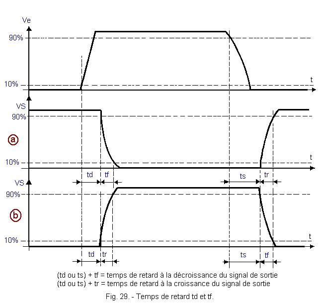
It is now necessary to approach the problem of the reaction and transit times of these fixtures.
Let's go back to the NAND circuit. Let's place one of its entries at the high level and see what happens at the exit, when its second entry goes from one state to another.
For convenience, refer to Figure 29-a.
Starting from a steady state at the output (here a high state) and after the appearance of the high level at the input Ve, we see a delay time td (delay-time) before the output signal reacts. This delay corresponds to the time of modification of the loads at the junctions.
Then, the output signal evolves exponentially during the time tf which corresponds to the fall-time. This evolution is characteristic of an RC circuit that discharges (resistance of the semiconductor material and parasitic capacitances). This zone corresponds to the passage on the right of charge from one rest point to the other. This is the zone of amplification and instability.
Follow a bearing which corresponds to the second stable state. As long as input Ve is not changed, the output retains this state.
After deleting the input signal, there is a delay time ts (storage-time) due to the time of modification of the charges at the junction.
Finally, the rise to the high start state tr (rise-time) which is performed according to an exponential variation corresponding to the load of the RC circuit previously mentioned.
The tr and tf zones correspond to the movement on the charging right of the operating point from A to B or the opposite (that is to say the blocking of saturation or vice versa).
We have seen that the transit speed from one point to the other is limited by the junction capacities (plus the parasitic capacitances), which is clearly shown in Figures 29-a and 29-b. These times (tf and tr) are measured between 10% and 90% of the signal value.
Figure 29-b shows the output signal for an AND circuit.
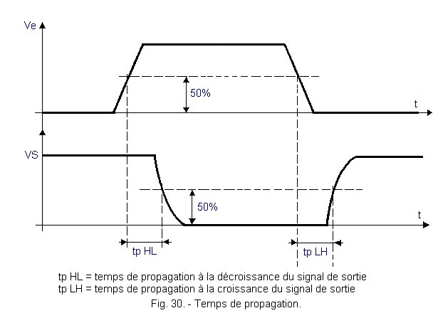
For simplicity, the builders indicate :
the delay at the decay of the output signal : tpHL.
the propagation time to the growth of the output signal : tpLH
Figure 30 illustrates those times which are measured from a variation of 50% of the input or output signal and with an output load which is defined (in principle for the TTL, consists of a capacitance of 15 pF in parallel with a resistance of 100 to 400 Ω.
For the NAND circuit taken as an example, we would find :
tpHL
between 7 and
15
ns (ns = 10-9
seconde).
tpLH
between 11 and
22 ns.
This for an output load of 15
pF and
400 W.
Finally, the maximum power consumed by the entire housing, which may contain several operators, is indicated on the records. This data is not negligible because it allows to determine the power of the power supply.
It must be kept in mind that the proper functioning of electronic assemblies is closely linked to the qualities of their power supplies. With regard to the logic circuits, these will have to be able to withstand large variations of current in very short times (change of state totem-pole assemblies). Decoupling, near boxes, will have to be put in place.
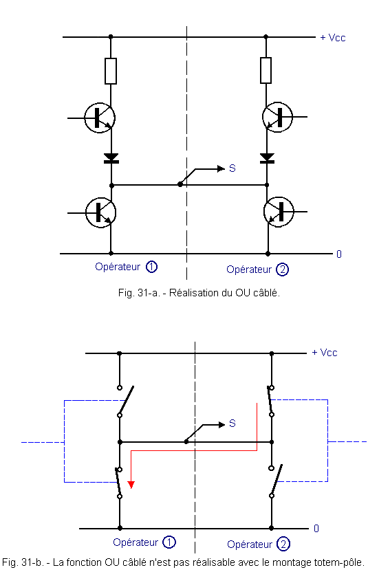
It is interesting, in assemblies, to minimize the number of modules, either for cost reasons or for operational reasons (in order to balance transfer times between two paths).
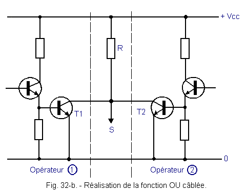
For example, if you combine the output of two operators, by wiring, you get the function :OR wired.
With totem-pole editing, this meeting is not possible.
Figure 31 illustrates why this procedure is not possible (short circuit of the power supply).
Manufacturers build operators designed for this purpose and take the name of operators
open collectors.
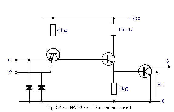
These allow the wired OR function. Figure 32-a shows an open-collector NAND circuit.
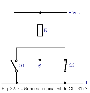
Figure 32-b illustrates the procedure and Figure 32-c shows the operation by substituting the output transistors with switches (S1 and S2).
The common resistance to the collectors of the output transistors must be placed externally.
In this case, there is no short circuit on the power supply, regardless of the position of S1 or S2.
Their parallel connection shows that it is the OR function.
In TTL technology, it must be remembered that this function is only possible when the operators are output : open collector (and by externally wiring the common collector resistance R).
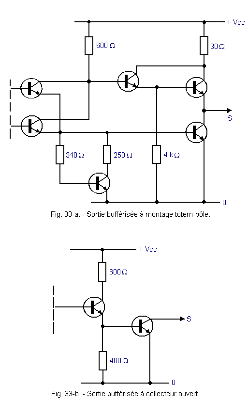
It is sometimes necessary to order more than ten operators with an output.
In this case, operators are used whose output can inject or absorb more current. These operators are said to have buffered output. Some only perform this function, in this case they are called buffers.
This output can be totem-pole mount with a series resistance of 30 Ω instead of 130 Ω and the output transistors are likely to withstand a higher current. Their polarization is a little different and the diode is removed.
It can also be open collector with a more powerful output transistor (more powerful collector current and higher VCE).
Figures 33-a and 33-b show these two mounts.
There are several variants of the TTL.
Their purpose is to reduce the consumption (TTL - L, L = Low-power) but at the expense of the operating speed (only 3 MHz ),
an increase of this speed (120 MHz) as well as the consumption (TTL - S, S = Schottky).
Another variant of the TTL is TTL - LS (Low power Schottky) technology. It has the same speed of operation as the conventional TTL (about 45 MHz) but a consumption 5 times less. She is supplanting the TTL.
It should be noted, in addition, the tri-state TTL (3 states). In addition to the two logic states, a third intervenes to disconnect the operator from the rest of the assembly by putting the two output transistors of the totem-pole in the off state (OFF state) or high impedance.
This way of proceeding was born as a result of the data bus technique.
A large number of operators connected to these lines led to the use of wired OR, and therefore open collector operators.
The latter being much slower than the totem-pole assembly, the idea was to keep the latter but by disconnecting from the line, all operators not concerned by the transmitted signals, using a signal applied to a signal. special input and that blocks the two output transistors of each of these operators.
With the realization of the logical functions in TTL technology, ends this last TECHNOLOGY 2.
The following will deal with these functions but in MOS technology.
We will also discuss the various other technologies as well as the manufacturing processes of these circuits.
These headings are perhaps not among the most attractive, but we insist on the fact that technology is of great importance for the electronics engineer, both in terms of the choice of material and the understanding of transient phenomena.


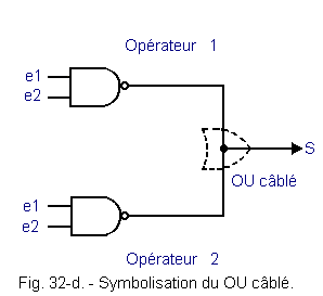
 The function OR Wired
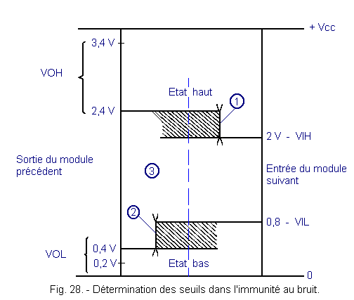
 Click here for the next lesson or in the summary provided for this purpose.
 Top of page
 Next Page