Examination of an OR Circuit (74C32) and a NOR Circuit (74C02) :
3.
- FIRST EXPERIENCE :REVIEW OF A CIRCUIT OR
With the following exercise, you will be able to check the operation of an OR circuit and establish the operating table and the truth table.
For this, you will use the integrated circuit MM 74C32 whose circuit diagram is shown in Figure 5. As you can see, this integrated circuit includes 4 OR circuits. The experiment concerns the examination of the first OR circuit whose inputs are connected to pins 1 and 2 and the output to pin 3.
The other 3 OR circuits contained in the integrated circuit have the same operating characteristics as you can check it yourself if you want by repeating the same tests.
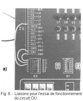
To do this experiment, follow the instructions below and refer to Figure 6-a.
a) Remove from the group of connectors all the links possibly present relating to the preceding tests.
b) Make sure that the battery is disconnected, then take the integrated circuit MM 74C32 and insert it into the ICX holder after straightening the legs if necessary, with the precautions of use recommended in the previous practices.
c) Using two pieces of 5 cm duly prepared wires, connect pin 1 of the integrated circuit with contact SW0 and pin 2 with contact SW1.
d) Using the 10 cm piece of wire, connect leg 3 of the integrated circuit with contact L0.
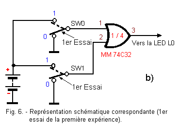
With these links, the input 1 of the OR circuit is connected to the common contact of the switch SW0 while the input 2 is connected to the common contact of the switch SW1 ; the output of the OR circuit is connected to the indicator L0.
The two switches are used to connect the two inputs to ground (0 V, low level L) or to the positive supply voltage (+ 4.5 V, level H), depending on whether they are respectively set to 0 or on 1.
e) Set the two switches to the 0 position ; the two inputs of the OR circuit are thus both connected to the ground, and are therefore at the level L. In this way, you have realized the schematic circuit in Figure 6-b (first test).
Now power the circuit by connecting the red and black cords to the battery and observe the L0 LED ; it is off, indicating a level L.
With this test, you found that in an OR circuit, when both inputs are low (in the L state), the output is also low (in the L state).
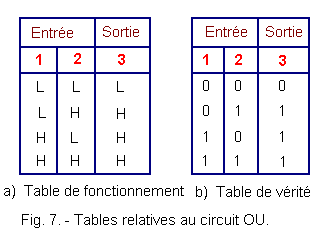
So you can draw up a table with two columns, the first reserved for the levels of the entries and the other relative to the level of the output.
On this table, you can report the result of the first test and therefore note L for input 1, L for input 2 and L for the output thus completing the first line of the operating table of the OR circuit.
f) Now switch switch SW1 up to position 1.
The input 2 of the OR circuit is thus brought to the level H. By observing the LED L0, you see that it is lit, which indicates that the output of the OR circuit is at the level H (high).
In the second row of the operating table, you can enter the following notes : L for input 1, H for input 2 and H for output.
g) Toggle switch SW0 to position 1 and return switch SW1 to position 0.
Under these conditions, entry 1 was raised to level H while entry 2 was brought back to level L.
By observing the LED L0, you see that it is always on, a clear sign that the output is still in state H.
On the basis of this test, you can fill the third row of the operating table by indicating that for the input H and L levels, the output is in the H state.
Return SW1 to position 1 again ; under these conditions both inputs are at a level H.
By observing the LED L0, you see that it is lit which indicates that the output is also at level H.
From this result, you can enter the last line of the operating table of the OR circuit (shown in Figure 7-a) by setting H to both inputs as well as to the output.
You can move from the operating table to the truth table by replacing the letter L by the symbol 0 and the letter H by the symbol 1, according to the positive logical convention. This will give you the table shown in Figure 7-b.
From the operating table of Figure 7-a, we can deduce that the output of an OR circuit is high when at least one of its inputs is in the high state, while the output is in the L (low) state only when its inputs are in the L (low) state.
The purpose of this experiment is to find that a NOR circuit is equivalent to an OR circuit followed by an inverter.
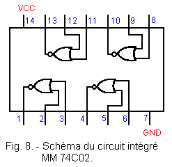
For this exercise, you will use the integrated circuit MM 74C02 containing 4 NOR circuits as you can see in the wiring diagram of Figure 8.
As usual, the test run will be performed on the first NOR circuit, that is to say the one whose inputs are pins 2 and 3 and the output pin 1.
Proceed as follows :
a) First make sure that the power supply is disconnected and remove the connections made in previous tests.
b) Remove the integrated circuit MM 74C32 from the support and insert in its place the integrated circuit MM 74C02.
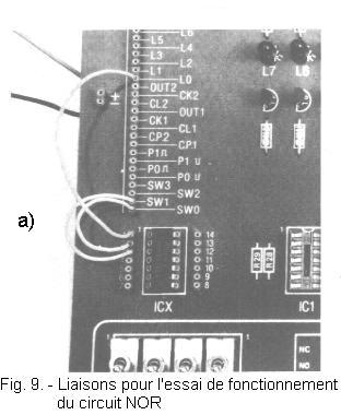
c) With the three pieces of wire used in the previous experiment, connect the points shown below and shown in Figure 9-a :
pin 1 of the integrated circuit MM 74C02 and contact L0,
pin 2 of the integrated circuit MM 74C02 and contact SW0,
pin 3 of the integrated circuit MM 74C02 and SW1 contact.
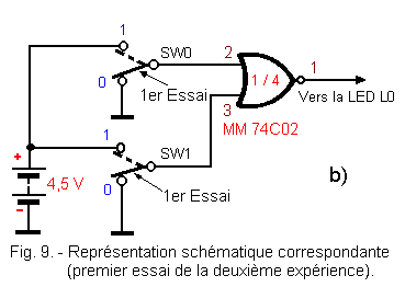
d) Set the two switches SW0 and SW1 to the 0 position.
Under these conditions, the two inputs of the NOR circuit are both at the L level and you have realized the circuit shown in Figure 9-b (first test).
Now power the circuit and observe the LED L0 : it is on. That is, when the inputs of the NOR circuit are in the LL state, that is both at a low level, the output is in the H (high) state.
e) Set switch SW1 to position 1, then put it back to position 0 and set SW0 to position 1. So you make both combinations LH and HL on the inputs. You notice that in both cases, the LED L0 remains off indicating that the output is in state L.
f) Finally put the two switches SW0 and SW1 on position 1. In this case also, LED L0 remains off indicating that the output is still in state L.
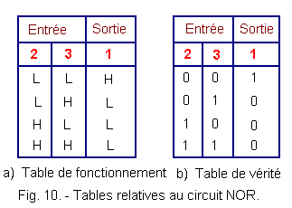
The results of these tests are summarized in the operating table illustrated in Figure 10-a, while Figure 10-b represents the corresponding truth table.
Thanks to the operating table of Figure 10-a, we can see that the output of a NOR circuit is at a high level only in the case where its two inputs are each at the level L (low). If only one of the two inputs where both are high, the output is at L (low).
By comparing the truth table of the NOR circuit (Figure 10-b) with that of the ORcircuit shown in Figure 7-b, you will notice that the first can be drawn from the second by a simple inversion, replacing each 0 by 1 and each 1 by a 0 in the output column.
This is an important point to make.
In the development of the truth table, so far, reference has been made to the positive logical convention, that is, the truth table has been drawn from that of operation by associating the value logic 1 at level H and logic value 0 at level L.
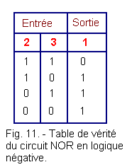
Let's see what happens when we operate according to the negative logic convention, that is to say if the logical value 1 is associated with the level L and the logic value 0 with the level H, in the case of the NOR circuit considered previously. The result obtained will be the new truth table represented in Figure 11.
Comparing this table with the truth table of the NAND circuit taken from the previous theory (See Digital Electronics, 3rd lesson), you will see that they are identical. We can conclude that a NOR circuit operating in negative logic is equivalent to a NAND circuit operating in positive logic.
It is therefore very important to remember the following :
The operating table of an integrated circuit describes the physical operation in terms of voltage levels.
The truth table, on the other hand, describes the logical function that it can perform, and which may be different depending on whether the logic adopted is positive or negative. To deepen the question, you will find further explanations in the Digital Electronic Theories (not to be neglected).


 Review of a NOR circuit
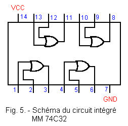
 Click here for the next lesson or in the summary provided for this purpose.
 Top of page
 Next Page