Morgan's Theorem - Positive Logic and Negative Logic :
2. - NEGATIVE LOGIC
So far, we have adopted a convention called a positive logical convention ; it is the most used and we think it is better for everyday uses to stick to this convention.
2. 1. - RECALL OF THE POSITIVE LOGICAL CONVENTION
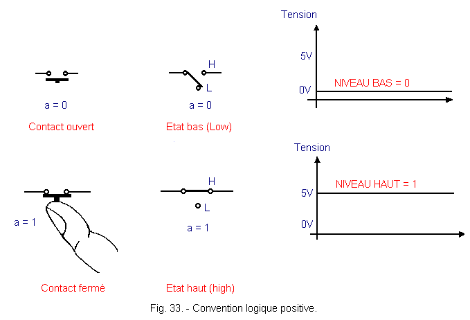
A closed contact (physical state), logical state 1 and an open contact (physical state) are mapped to logical state 0 (Figure 33).
2. 2. - NEGATIVE LOGIC
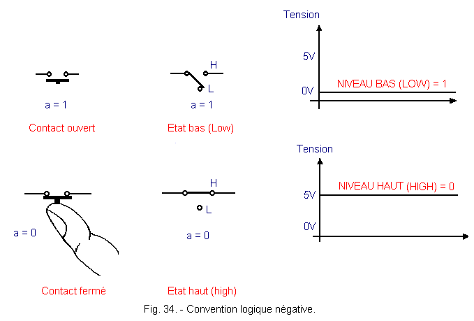
Only by convention, it has been decided to match the physical state open contact the logic level 1 and a closed contact the logic level 0 (Figure 34), that is to say the opposite of the usual convention.
Let's analyze what are the consequences of this change of convention.
PRINCIPLE OF DUALITY
Consider the operating table of an AND gate as given by the manufacturer (figure 35) in the case of an electronic AND gate :
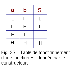
Let's now write the truth table of this montage, adopting the positive logical convention L = 0, H = 1 ; we get the truth table from Figure 36.
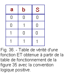
This truth table is the well-known truth table as we saw it in Theory 2.
Let's write again the truth table of the montage but this time, using the negative logical convention (Figure 37).
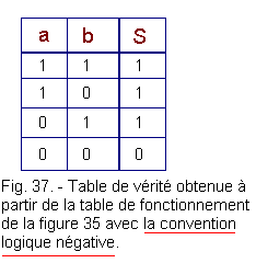
Let's now put this truth table in order so that the input variables grow in a binary order (Figure 38).
.gif)
inclusive OU.
We can therefore say that :
"An AND operator in positive logic behaves like an OR operator in negative logic".
If one establishes the truth tables of all logic circuits in both types of logic, one can write the following table (figure 39).
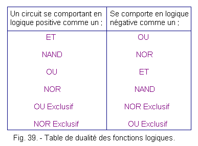
These correspondences were very used to save boxes in the digital circuits, but the fall of the prices of the circuits made practically abandon this system which is a source of errors.
On integrated circuit catalogs, the indicated function is the one that it would have in positive logic. An AND circuit therefore operates as an AND in positive logic and as an OR in negative logic.
In the rest of this theory, there will be no more than a positive logical convention, that is, the convention we have always used. Chapter 2 of this theory can therefore be considered a parenthesis. You will refer to this paragraph only in the unlikely event that you encounter an old system using the negative logical convention.
![]() 3. - THEOREMS OF MORGAN
3. - THEOREMS OF MORGAN
3. 1. - 1st THEOREM OF MORGAN ![]()
Demonstration by the circles of Euler Figure 40.
Let a set A and its complement ![]() (green hatches) and a set B and its complement
(green hatches) and a set B and its complement ![]() (red hatching).
(red hatching).
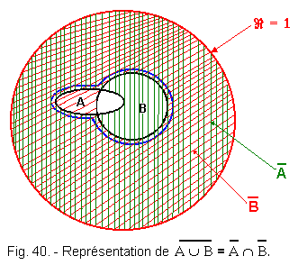
The meeting A È B of A and of B will be the area included in the blue outline.
The complement of
A
È
B
with respect to Â
will be the doubly hatched surface is ![]() .
This surface being doubly hatched, it goes of course that it is well the intersection of the complements of A and B is
.
This surface being doubly hatched, it goes of course that it is well the intersection of the complements of A and B is ![]() .
.
We can therefore say that :
![]()
So we can say in Boolean algebra that :
![]() =
= ![]() .
.![]()
The inverse of a logical sum of two variables is equal to the logical product of the inverses of these two variables.
3. 2. - 2nd THEOREM OF MORGAN ![]()
Demonstration by Euler circles (Figure 41).
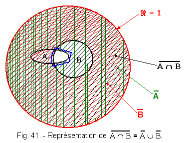
Let a set A and its complement ![]() (green hatches) and a set B and its complement
(green hatches) and a set B and its complement ![]() (red hatching).
(red hatching).
The intersection of A and B : A Ç B will be the area included in the blue outline.
The complement of A Ç
B is ![]() will be the hatched part in black.
will be the hatched part in black.
We also see that this same black hatched surface is the union of ![]() and
and ![]() is
is ![]() ,
indeed this black hatched area covers all the green hatching
,
indeed this black hatched area covers all the green hatching ![]() and all the red hatching
and all the red hatching ![]() .
.
In Boolean algebra, we can write :
![]() =
= ![]() +
+ ![]()
The inverse of the logical product of two variables is equal to the sum of the inverses of the two variables.
![]() 3. 3. - BACK
ON NAND AND NOR FUNCTIONS
3. 3. - BACK
ON NAND AND NOR FUNCTIONS
3. 3. 1. - NAND OPERATOR
In the previous chapter, we saw for the operator NAND, whose equation was ![]() ,
the following electrical circuit (Figure 42).
,
the following electrical circuit (Figure 42).
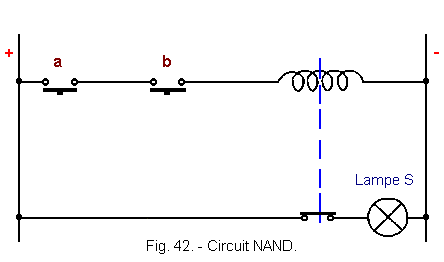
We can now thanks to the theorem of De Morgan simplify this circuit, indeed S = ![]() =
= ![]() +
+ ![]() .
It is therefore sufficient to put two contacts at rest in parallel to obtain the same result as before which is very interesting (Figure 43).
.
It is therefore sufficient to put two contacts at rest in parallel to obtain the same result as before which is very interesting (Figure 43).
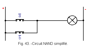
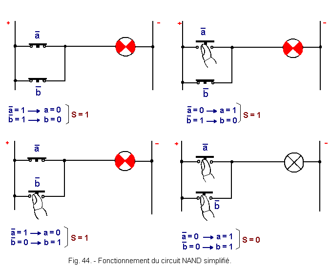
Let's check the functioning of this circuit (Figure 44) by studying the four possible combinations of a and b.
Let's put the results in a Karnaugh chart (Figure 45).
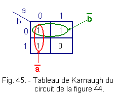
We find Karnaugh's painting of a NAND circuit (Figure 43).
We see in passing that the table of Karnaugh also gives S = ![]() +
+ ![]() and that thanks to him, we obtain the simplest solution.
and that thanks to him, we obtain the simplest solution.
3. 3. 2. - NOR OPERATOR
In the previous chapter, we saw the NOR operator whose equation was S = ![]() considering the De Morgan theorem we can write :
considering the De Morgan theorem we can write :
S =
![]() =
= ![]() .
.![]()
Hence the diagram of Figure 46 :
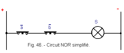
You will be able to carry out the verifications of the good conformity of the table of truth of this circuit NOR with the one that we know.
![]() 3. 4. - CIRCUIT
ASSOCIATION, SCHEMA TRANSFORMATION
3. 4. - CIRCUIT
ASSOCIATION, SCHEMA TRANSFORMATION
We have studied different fundamental functions that are available as integrated circuits.
In each case, there are several functions of the same type. Thus, there are integrated circuits containing four NAND with two inputs.
The designer of digital systems must therefore, when he has used a NAND know that in the same housing three other NAND two inputs are available and still unused.
It will therefore sometimes be interesting to be able to transform an AND circuit into two NAND circuits, for example if there is an excess of available NAND gates when it would be necessary to add an additional box containing ET.
The problem is complicated when one wants to make for example an OR with NAND. We then resort to a simplification by means of De Morgan's theorem.
De Morgan's theorem gives us the following relation : ![]() =
= ![]() +
+ ![]() which makes it possible to develop equivalences between circuits.
which makes it possible to develop equivalences between circuits.
If we observe the first term of equality, that is to say ![]() ,
we note that it is the result obtained at the output of a NAND from two variables a and b present on the entries.
,
we note that it is the result obtained at the output of a NAND from two variables a and b present on the entries.
The second term of equality ![]() +
+ ![]() represents a logical sum, that is to say the result obtained at the output of an OR whose inputs have been complemented.
represents a logical sum, that is to say the result obtained at the output of an OR whose inputs have been complemented.
The schematic representation of this equality is shown in Figure 47.
This means that a NAND is equivalent to an OR preceded by inverters.
To check in practice that the two previous montages are well equivalent, it is enough to apply logical levels in a and b to the second assembly to see if one can write a truth table analogous to that of a NAND circuit. In this case, the two montages will be equivalent.
We know that there are 4 different combinations of two variables a and b ; if you wish, you can check for these four combinations. We will study for our part only the combination a = 0 and b = 0.
Figure 48 shows the result for a = b = 0. Knowing the truth tables of the inverters, that of the AND and that of the OR, it was easy for us to find this result.
The level of the output is then 1 for both montages.
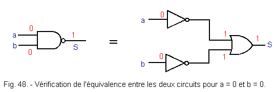
By proceeding in the same way, we can verify that the equivalence is valid when a = 0 and b = 0, a = 1 and b = 0 and finally when a = b = 1. We thus find the truth table of a NAND.
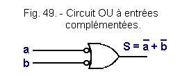
The OR circuit with complemented inputs can be represented as shown in Figure 49.
Example :
Apply this principle to the scheme of Figure 50.
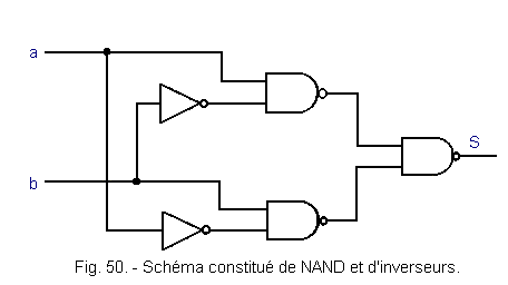
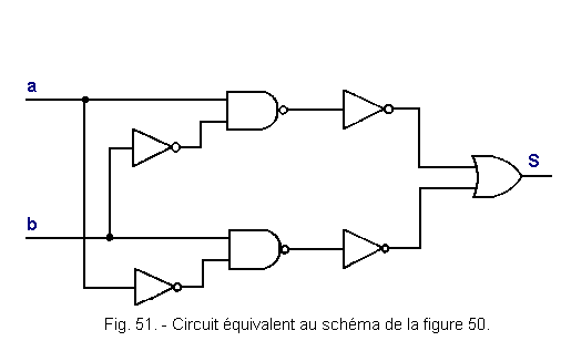
To see how it works, it is transformed into an equivalent circuit by applying DE MORGAN's theorem to the output NAND circuit.
We get Figure 51.
We now see that each NAND circuit is followed by an inverter, which amounts to replacing the NAND and the inverter with an AND. Indeed, we can say that ![]() = y (two successive inversions are canceled).
= y (two successive inversions are canceled).
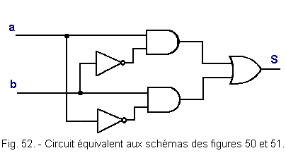
The logic circuit of Figure 52 is thus obtained.
The circuit is none other than that of an exclusive OR already presented Figure 25.
DE MORGAN's theorem allowed us to find an equivalent circuit. We will see later how to take advantage of it in other examples.
From now on we can see that any logic circuit can be realized with only circuits of the same type, NAND for example.
The circuit designer always has the possibility to choose at his convenience the type of housing he wants to use.
So far, we have applied DE MORGAN's theorem to NAND circuits, but it can be applied in a general way to any logical equation and in particular to the NOR function.
In the latter case, the relation is
![]() =
= ![]() .
.![]()
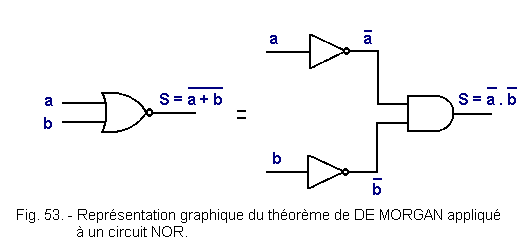
We can materialize this equality by the scheme of Figure 53.
If you wish, you can easily by taking the same principle as for the demonstration of the equivalence schematically Figure 47 (case of the NAND) establish the table of truth of each of the assemblies Figure 53 to demonstrate the equivalence of these.
End of this lesson and we will learn the QUINE-MAC CLUSKEY Method.
 Click here for the next lesson or in the summary provided for this purpose. Click here for the next lesson or in the summary provided for this purpose. |
|
 Previous Page Previous Page |
 Next Page Next Page |
Nombre de pages vues, à partir de cette date : le 27 Décembre 2019
Envoyez un courrier électronique à Administrateur Web Société pour toute question ou remarque concernant ce site Web.
Version du site : 10. 4. 12 - Site optimisation 1280 x 1024 pixels - Faculté de Nanterre - Dernière modification : 02 Septembre 2016.
Ce site Web a été Créé le, 14 Mars 1999 et ayant Rénové, en Septembre 2016.
 DE MORGAN theorems
