5. - OPERATING TESTS OF THE INTEGRATED CIRCUIT MM 74C08
With the following experience, we will experimentally verify the operation of an integrated circuit with four doors AND, type MM 74C08 or equivalent, and you will see in particular that an AND circuit can be used to allow or prohibit the passage of a binary signal according to the state of a control input.
You will practice check the operating table and the truth table of the circuit in question.
5. 1. - PRELIMINARY CONNECTIONS
a) - Remove all the links made in the previous experiment.
b) - Remove the integrated circuit MM 74C04 from the ICX support ; to do this, proceed as follows :
gently thread the blade of a screwdriver between the IC housing and the bracket.
turn the screwdriver : the integrated circuit is lifted as seen in the picture of Figure 20.
by levering gently with the screwdriver to avoid deforming the pins of the integrated circuit, remove it completely from the support.
c) - Insert the integrated circuit MM 74C08 into the ICX socket, observing the precautions given when mounting the first integrated circuit.
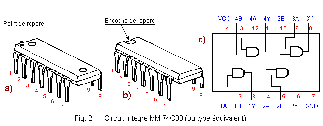
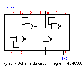
As can be seen in the diagram shown in Figure 21-c and provided by the manufacturer, the integrated circuit MM 74C08 contains 4 AND circuits having identical characteristics but operating independently of each other. However, they have a common diet.
For this integrated circuit (as indeed for all integrated circuits in general) the numbering of the pins corresponds to the view from above ; pin 1 is the one near the reference point (Figure 21-a) or to the right of a semicircular notch made on one of the short sides of the housing, as shown in Figure 21-b.
5. 2. - SECOND EXPERIENCE : EXAMINING A CIRCUIT AND
The following experiment concerns the first AND circuit whose two inputs are pins 1 and 2 while the output is pin 3.
As already indicated, the other three AND circuits contained in the integrated circuit operate in the same way. So you can easily check them by repeating the same tests.
The experiment consists in connecting the output of the AND circuit to the LED indicator, L0 in order to record the output voltage levels corresponding to the different combinations of possible voltage levels on the inputs.
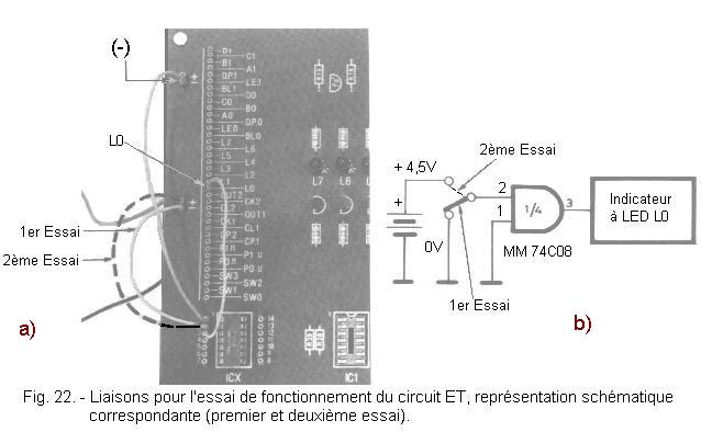
Perform the operations in order by referring to Figure 22.
a) - Prepare a new piece of insulated rigid wire of approximately 15 cm and connect the first input, pin 1, of the circuit AND to the contact marked "-" at the top left of the set of connectors. Through this link, the input is put at the potential of the mass.
b) - Using the wire you have prepared (length of your choice), connect the second input of the AND circuit, pin 2, to the other contact marked "-" as shown in figure 22-a ; this input is thus grounded.
c) - Using another piece of wire, connect the output, pin 3, of the AND circuit to the input of the LED indicator marked with the symbol L0 on the connector group.
Through these links, you have realized the circuit shown in Figure 22-b (first test).
You can power the circuit and observe the LED L0 : it remains off. You will notice that : when the inputs of the AND circuit are both at the low voltage level, that is to say L, the output is also at the level L.
d) - Disconnect the power supply and now connect input 2 to the contact indicated by the "+" sign, as shown in dotted line Figure 22-a. In this way, the second input is no longer at a low voltage level (0 V), but at a high voltage level (+ 4.5 V).
The electric circuit relating to the new links is also represented in Figure 22-b (second test).
Feed the circuit again and observe the LED L0 : it remains off. So you notice that : when one input of the AND circuit is in the H (high) state and the other in the L (low) state, the output stays in the L state.
For convenience, the two experiments of the experiment were represented in a single figure ; on the first test, input 2 is connected to ground and is at level L, while at the second test it is connected to the + 4.5 V voltage and is then at level H.
From these two experiments, you can deduce that, if one of the two inputs (in our case the input corresponding to pin 1) is at a low level, the level that can take the other input has no influence on the output.
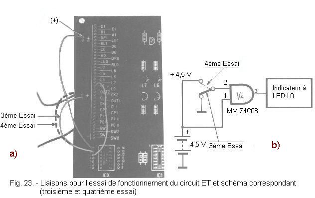
e) - Now connect the input 1 of the integrated circuit to the "+" contact, that is to say the high level and keep it in this position, repeat the two previous tests by connecting the input 2 first to ground on the "-" contact, as shown in figure 23-a (third test), and then on the "+" contact, as shown in dotted line on the same figure (fourth test). Figure 23-b shows the circuit diagram of the realized circuit.
The procedure is always the same :
unplug the power
make the connections
reconnect power
observe the LED L0.
You notice this time that the input 1 being at a high level, the output takes the same level as that of the entry 2, that is to say that it takes a low level (L) if the level of input 2 is low (L) or goes high (H) if the level of input 2 is high (H).
This is the characteristic operation of an AND circuit which can thus be used to control the transmission of a binary signal.
In this case, the input 1 is called the control input, because if this input is at the level L, the output is insensitive to the variations of the level present on the input 2 ; while if the input 1 is at the level H, the output takes the same level, high or low, as that present on the input 2.
Of course, the two inputs being symmetrical, they are interchangeable, and the input 2 can become the control input if it is brought to the level H ; in this case, the output will assume the state corresponding to that of input 1.
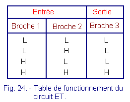
The tests carried out give you all the data needed to establish the operating table of the AND circuit. For example, you noticed that with both inputs at L, the output is at L level.
You could then check for all other voltage level combinations on the inputs the output voltage levels by observing the L0 LED.
Transcribe the results obtained in the OPERATING TABLE shown in Figure 24.
Looking at this table, you can conclude that in an AND circuit, the output is at a high level (H) only when the inputs are both high (H) ; if either or both inputs are at a low level (L), the output is at a low level (L).
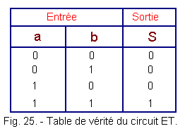
From the operating table, the truth table can be established by associating the logical value 0 and the level H with the logic value 1 as shown in Figure 25.
In this table, the two inputs named a and b and the output S are designated by the corresponding pin numbers, because in digital circuit catalogs, the truth table is usually presented in this form.
This table describes the logical operation of the AND circuit. Output S is in logic state 1 only when both inputs a and b are both in logic state 1.
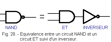
The integrated circuit MM 74C00 contains 4 NAND circuits as shown in Figure 26. With the following experiment, you can see that a NAND circuit behaves like an AND circuit followed by an INVERTER.
6. 1. - THIRD EXPERIENCE : EXAMINING A NAND CIRCUIT
a) - Disconnect the power supply and remove all connections made during the last experiment.
b) - Remove the integrated circuit MM 74C08 from the ICX test stand and insert the new integrated circuit MM 74C00 into it.
Now you can start the test run of the first NAND circuit (its inputs are pins 1 and 2 and the output pin 3). You will proceed in exactly the same way as for the previous experiment conducted on the AND circuit.
By carrying out the four possible combinations of states of the inputs of the NAND circuit, note the state of the output by observing each time the LED L0.
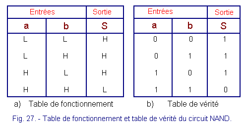
Using the results obtained, you can establish the operating table and then the truth table of the NAND circuit. These two tables are shown in Figure 27.
By comparing the operating table of the NAND circuit with that of the AND circuit, you can see that the output levels of the NAND circuit can be obtained starting from those of the circuit AND by a simple inversion, that is to say by replacing in the last column relative to the output, H by L and vice versa.
This confirms that a NAND circuit is equivalent to an AND circuit followed by an inverter, as shown in Figure 28.
c) After completing the experiment, remove the MM 74C00 IC from the holder and replace it in the graphite foam. With this practice, you have completed the mounting of the LED indicator and its test.
Using the LED indicator to visualize the high and low voltage levels at the output of a digital integrated circuit, you have analyzed the operation of some integrated circuits including inverters, AND circuits and NAND circuits.
In the next practice, you will continue wiring the printed circuit board and you will examine the operation of other types of circuits.
The various tests carried out with transistors and LED diodes have not yet been theoretically explained, these are given in the new lessons of TECHNOLOGY 1 which deals with semiconductors, (these lessons are very important to understand the digital system, so do not neglect).
It will be interesting when you examine this technology to come back to practice N° 2 to better understand.
The sequence of the program may seem illogical to you but in reality it is motivated by the unfolding of the practices and you will be able to see after having read five or six theories and five or six practices that these complement each other and make it possible, thanks to some returns in back, to make revisions in order to understand the important points.


 Function tests of the integrated circuit MM 74C00 "NAND"
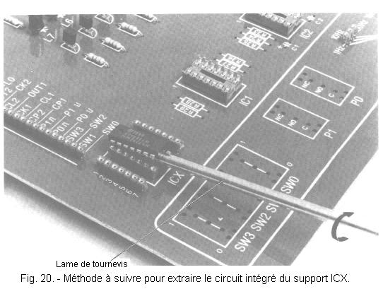
 Click here for the next lesson or in the summary provided for this purpose
 Top of page
 Next Page