4. - CHECKING THE OPERATION OF THE INTEGRATED CIRCUIT MM 74C04
As a first experiment, check the operation of an integrated 6 inverters circuit by raising the high (or State high) and low (or State low) voltage levels present at the input and output of an inverter using of the LED indicator.
Let's first look at what are the characteristics of this integrated circuit.
4. 1. - DESCRIPTION OF THE INTEGRATED CIRCUIT MM 74C04
With the first set of hardware you have purchased or you have an integrated circuit marked MM 74C04 or equivalent, as shown in Figure 13-a.
In the diagram of Figure 13-b, it can be seen that the pin 1 corresponds to the input of the first inverter, while its output leads to the pin 2. The pins 3, 5, 9, 11, 13 constitute the inputs five other inverters whose outputs respectively correspond to the pins 4, 6, 8, 10, 12.
The six inverters are independent of each other although they are contained in a single housing for the sake of economy and for the purpose of miniaturization.
By cons, their power is common : we must apply a positive voltage between + 3 and + 15 V on pin 14 marked Vcc (for collector voltage) or sometimes with the symbol VD or VDD (for voltage drain) ; On the other hand, it is necessary to connect to ground GND pin 7 (for ground or terre in French) or sometimes VSS (for source voltage).
This range of supply voltage between + 3 V and + 15 V is characteristic of the integrated circuits that you will use for experiments and in general for a large part of the integrated circuits of the CMOS family.
Other integrated circuits belonging to the TTL family require, on the other hand, a supply voltage of + 5 V with a tolerance of ± 5% ; for these circuits, a voltage greater than 5.5 V would certainly be destructive, while a voltage value lower than + 4.5 V could not guarantee correct operation.
4. 2. - FIRST
EXPERIENCE : STUDY OF AN INVERTER CIRCUIT
With this experiment, you will study the operation of the first inverter contained in the integrated circuit whose input is connected to pin 1 and the output to pin 2
The other five inverters included in the same integrated circuit have exactly the same operation of the first. You can check them yourself one after another if you want, by repeating the same operations.
The test consists in connecting the output of the inverter in question to the LED indicator, L0 and to see what voltage levels are obtained at the output according to the voltage levels present at the input.
On the basis of these results, you will establish the operating table and the truth table of the inverter.
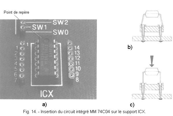
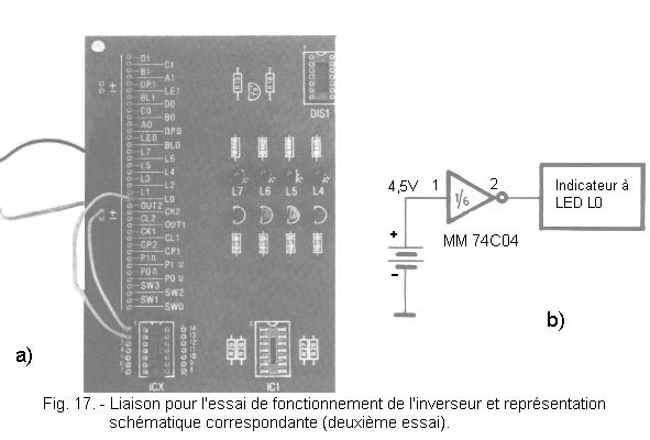
Now remove the MM 74C04 integrated circuit from the graphite foam and insert it into the ICX test holder, orienting it correctly as shown in Figure 14-a and following the instructions below :
a) - Before inserting the integrated circuit into the holder, carefully examine its pins ; if one of them is bent, gently straighten it with tweezers.
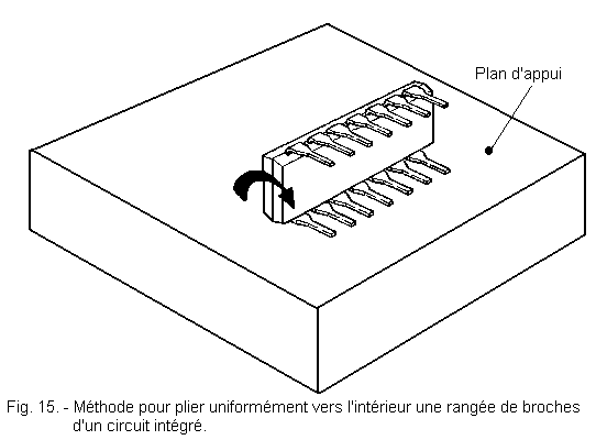
b) - Present the integrated circuit on the bracket and verify that the pins match the holes in the bracket ; if it is not the case, that is to say that the pins of the integrated circuit are slightly shifted (as shown in Figure 14-b), you must straighten them. To do this, lay the circuit on a hard surface and apply adequate pressure to bend the pins evenly inwards, as shown in Figure 15. The same operation must be performed on the other side of the integrated circuit, so that the two rows of pins are folded symmetrically with respect to the housing.
c) - The pins of the integrated circuit facing the holes of the support (Figure 14-c), press gently but firmly on the integrated circuit to plug into the support.
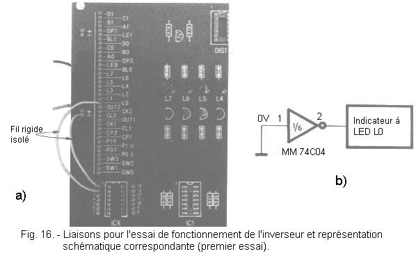
d) - Following the instructions given above, prepare two pieces of insulated tinned wire about 10 cm each to establish the connections between connectors.
e) - Using one of these wires, connect the output of the inverter, that is to say pin 2 to the input of the LED indicator marked by the symbol L0 of the group of connectors.
f) - With the other wire, connect the input of the inverter, see pin 1 to the "-" contact of the connector group.
The connections made are shown in Figure 16-a and with them you have made the circuit shown schematically in Figure 16-b.
As you can see, the links relating to the supply voltage are not represented in this circuit, its value is not indicated either : this is a convention generally adopted in the representation of the diagrams of the logic circuits. It remains, however, of course that the supply voltage must, in each case, be present and have an appropriate value for the circuits supplied.
In Figure 16-b, the LED indicator circuit is simply represented by a rectangle, since it is not part of the logic circuit itself, but is used only as a control device. This rectangle thus represents the LED indicator circuit, L0 with the corresponding control transistor, whose complete diagram has already been given in Figure 12.
You can see inside the graphic symbol of the inverter the indication 1 / 6 which means that the diagram represents one of the six inverters included in the same integrated circuit. However this fraction is often omitted for the sake of simplification.
The number of the spindle is transferred to the input and output of the inverter. This indication is always on the diagrams of the logic circuits. It is very useful for their understanding in view of their practical realization.
g) - After checking the accuracy of the connections made, feed the circuit : that is to say, connect the red and black alligator clips to the battery respecting, of course, the polarities as you know how to do now. You notice that the LED L0 lights up.
h) - Disconnect the battery. Remove the wire from the "-" contact and insert it into the "+" contact, as shown in Figure 17-a. You thus realize the circuit of figure 17-b. Feed the circuit again. You notice that the LED L0 goes out.
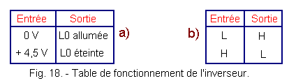
Figure 18 summarizes in the form of a table the result obtained. The first column (input) contains the low (0 V) and high (4.5 V) voltage levels applied to the inverter input. In the second column (output) are the corresponding states of the LED indicator L0 connected to the output of the same inverter.
Remember that the status of the LED indicator means :
LED on = high voltage level
LED off = low voltage level
Consider that a high voltage level is conventionally represented by the letter H (initial of the English word High, that is, high) and a low voltage level by the letter L (initial of the English word Low meaning low). The table of Figure 18-a can be converted to that of Figure 18-b called the OPERATING TABLE of the inverter.
Finally, we can conclude on the basis of this table that the output level of an inverter is always the opposite of that of the input, or that a low input level corresponds to a high output level. and vice versa.
The first experiment completed, disconnect power from the circuit.
4. 3. - TABLE OF TRUTH OF THE INVERTER
You will see in Theory N° 3 that circuits working with two levels, high (positive voltage) and low (zero voltage) signals like the ones we have, can provide two distinct logical functions depending on whether one operates in logic positive or negative.
According to the positive logical convention which is the most used, at the low level L is associated the logical state 0 and at the level H the logical state 1.
To define the characteristics of a digital type component, IC manufacturers generally provide the operating table, sometimes the truth table or both.
To conclude, it should be noted that if we represent by the letter a the input signal, that is to say the input variable (1 or 0) and by the letter S the output signal d'an inverter, the relation binding a and S can be written in the following form :
S =
where the bar above the letter a indicates the inversion of the logical output state relative to that of the input.
We will continue to deepen the other two integrated circuits namely MM 74C08 and MM 74C00 on another page so as not to clutter it.


 Study of an inverter circuit
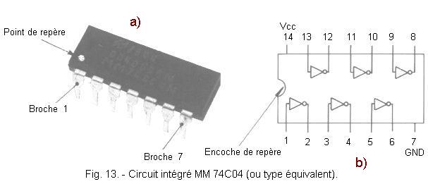
 Click here for the next lesson or in the summary provided for this purpose.
 Top of page
 Next Page