 Ramp converter
Converter Errors with Successive Approximations - Ramp Converter :
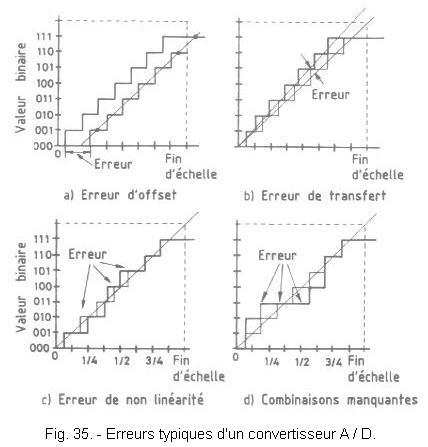
3. 4. - CONVERTER ERRORS WITH SUCCESSIVE APPROXIMATIONS
The A / D converter may be subject to the same errors as the D / A converter ; offset error, transfer error, linearity error.
If the latter is excessive, it may happen that some combinations are simply «skipped». Figure 35 shows the effects of these various errors on the transfer curve of the converter.
There is another possibility of error, due to the variations of the signal to be converted, which until now has been considered fixed.
Usually, this does not happen that way. Figure 36 illustrates the process when the Vx signal varies during the conversion.
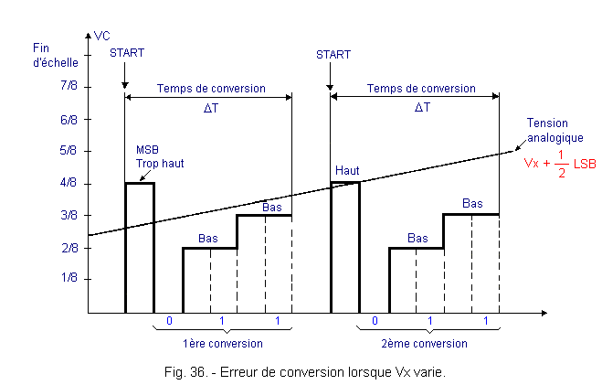
The voltage to be converted Vx changes from 3 / 8 VR at the beginning of the first conversion, to 5 / 8 VR after the second conversion, and yet both conversions give the same result (011).
It is therefore necessary that the signal does not change too rapidly. The maximum variation V allowed is a function of the reference voltage VR, the number of bits n of the converter, and the conversion time tconv according to the formula :
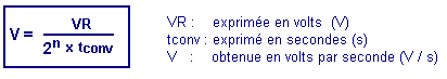
For a 10 bits A / D converter, working with a reference voltage VR = 10 volts and a conversion time of 0.1 seconds, we will have :
![]()
Thus the input signal can vary at most about 1 / 10 volts per second.
Fortunately, successive approximation converters are usually faster and convert to microseconds.
If the conversion time is 10 µs, we obtain :
![]()
Although this value seems high, in fact it is not. Indeed, 1000 V / s is equivalent to 10 volts in one hundredth of a second. Very often, the signals to be converted vary more rapidly.
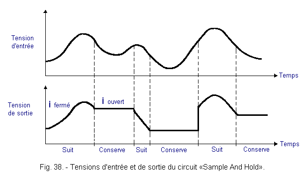
We must then resort to an artifice : to maintain the fixed signal during all the duration of the conversion, by means of a suitable circuit, called «Sample And Hold» in English, which means sampling circuit and maintenance.
The English word exactly writes the function of the circuit because it literally means «sample and preserve». Indeed, it takes on command a value of the analog signal and keeps it for the time necessary for the conversion.
Figure 37 shows a very simple «Sample And Hold» circuit. A capacitor C is connected to the «+» input of an operational amplifier mounted as a follower amplifier (gain = 1) and having a high input impedance.
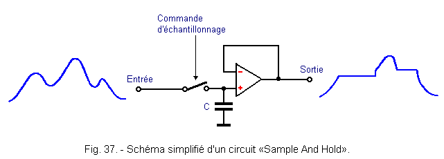
When the switch I is closed, the input signal is found, without modification, at the output of the amplifier, since the gain of the latter is equal to 1.
When you open the switch, the input signal has no influence. The capacitor C retains in the form of electric charge, the last value of input voltage existing before the opening of the contact. At the output of the amplifier, this voltage is found throughout the duration of opening of the switch. Indeed, the discharge of the capacitor C is insignificant since the input impedance of the amplifier is very high.
Figure 38 illustrates the operating principle of the «Sample And Hold» circuit.
An analog data processing chain usually includes an A / D converter associated with a «Sample And Hold» circuit, unless the signal to be converted is very slow.
The Figure 39 shows the example shown in Figure 36, but with the correction provided by a «Sample and Hold» circuit.
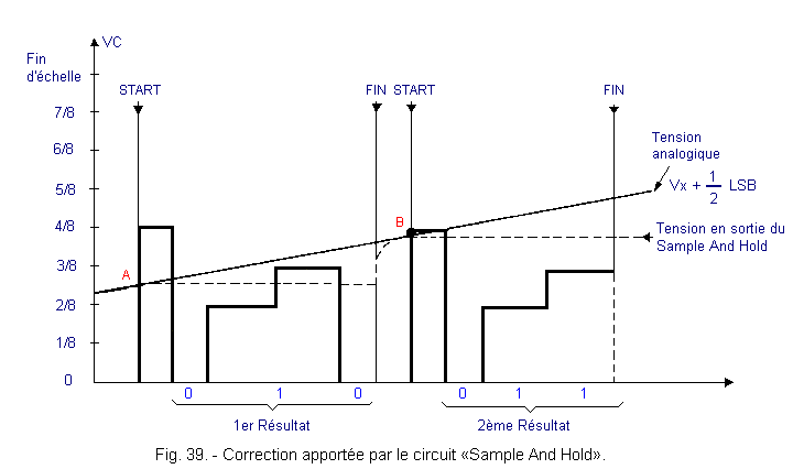
At points A and B, switch I, which was previously closed, is opened. It remains open for the duration of the conversion. The first conversion gives the value 010, but the second conversion indicates the value 011, which is closer to reality than that obtained from Figure 36.
![]() 3. 5. - RAMP CONVERTER
3. 5. - RAMP CONVERTER
Converters of this type are widely used for the construction of digital voltmeters and for measuring variables that vary slowly, such as temperature and pressure.
They are not suitable for converting rapidly varying signals.
The simplest possible ramp converter is shown in Figure 40. It consists of an RC circuit, a control circuit and a counter.
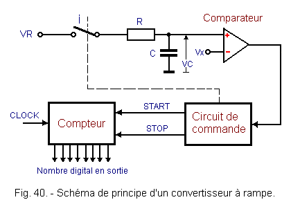
Before the conversion, the capacitor C is discharged and the switch I is open.
At the beginning of the conversion, the control circuit closes the contact I and starts the counter that starts counting the clock pulses.
Since I is closed, capacitor C begins to charge through resistor R.
If a sufficiently high voltage VR is used with respect to the voltages Vx to be converted, it can be considered that the load of C is comparable to a linear ramp (Figure 41).
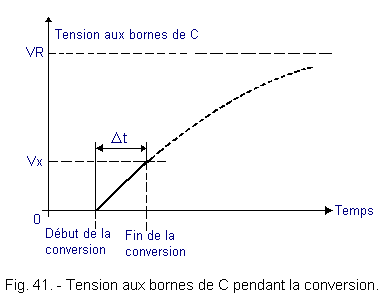
When the voltage VC across the capacitor reaches the value Vx to be measured, the comparator toggles and signals equality to the control circuit which immediately stops the comparator and opens the contact I.
The conversion is completed and the number of clock pulses that have been counted during the time Δt set by the capacitor to discharge to the value Vx can be read from the counter.
The higher the value of Vx, the longer the capacitor will take to load at this value.
Just design the counter appropriately, so that the totalized number directly gives the value of Vx in the desired binary code.
In reality, things are not so simple. Indeed, the accuracy of such a converter depends to a large extent on the capacitor and generally the capacitors are not very accurate.
We then resort to a more complex method called double-ramp conversion, where the accuracy does not depend on the capacitor.
This method illustrated by the graph of Figure 42 is based on the charge and the linear discharge of a capacitor (remember that the linearity of the charge or the discharge is obtained when these two operations are carried out with a constant current).
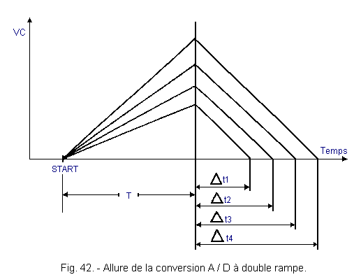
The voltage to be converted Vx is applied to a capacitor C, during a fixed time T, independent of the value of Vx.
The charge of C depends therefore only on Vx and is all the higher as Vx is large.
The slope of the ramp during the load of C is variable and depends on the value of Vx.
When charging is complete, the control circuit applies the reference voltage VR to the capacitor. This last voltage has a sign opposite to that previously applied and causes the discharge of the capacitor C.
The discharge is made with a constant slope equal to VR / RC.
When the voltage VC (across the capacitor C) reaches zero, the conversion is stopped. A counter measures the time Δt required to discharge the capacitor C and directly outputs the result of the conversion as a binary number.
The time Δt is directly related to the height of the charging voltage, which in turn depends on Vx.
Since capacitor C works in linear mode, we can say that the charge stored by C is proportional to Vx x T, while the load that C gives during the discharge is proportional to VR x Δt. Since the quantity of electricity sold by the capacitor is equal to that previously received, it can be deduced that :
Vx x T = VR x Dt from where Dt = Vx x (T / VR)
T and VR are constant and known terms since the beginning of the measurement. We can therefore conclude that Δt is directly proportional to Vx.
Figure 43 gives a schematic diagram of a double-ramp converter.
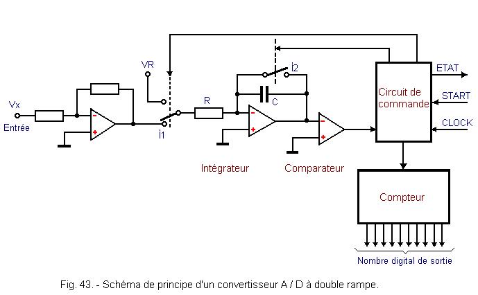
The input Vx is not directly connected to the network RC, but passes through a gain -1 operational amplifier. This inverter stage makes it possible to apply a signal of sign opposite to that of VR to the capacitor C and it also serves to separate the converter of the circuits that precede it.
The signal Vx is applied by the switch I1 to the resistor R and to the capacitor C.
The capacitor C is no longer connected between one of the terminals of R and the ground, but between the output and the input «-» of an operational amplifier. This assembly constitutes an integrating circuit which makes it possible to obtain a perfectly linear charge and discharge of the capacitor.
The control circuit alternately activates two switches. The first I1 at the beginning of the conversion is placed downwards and transmits the voltage Vx to the network RC, thus allowing the charging of C. After a fixed time T, the switch I1 is flipped upwards. The voltage VR, of sign opposite to Vx, is applied to the network RC and the discharge of C is carried out.
At the same time, the control circuit instructs the counter to start counting the clock pulses.
A comparator located after the integrator circuit makes it possible to detect the zero crossing of the discharge of the capacitor C. This information is sent to the control circuit which blocks the counter.
The second switch I2 is closed for a short time before the start of the conversion so as to bypass the capacitor C and thus eliminate any residual electric charge.
A double-ramp converter offers many advantages : The accuracy of the measurement is independent of the capacitor accuracy, furthermore, the linearity is excellent and there can be no missing combinations as in the case of the successive approximation converter. Finally, the resolution is limited only by the characteristics of the analog circuits (operational amplifiers) and can be very high. Add to this that any high frequency parasites are very well tolerated and generally do not give rise to erroneous indications.
To all these advantages, it is necessary to oppose a major disadvantage : it is the slowness of the conversion.
The counter must indeed start from scratch and count until the time T, then return to zero and then count the time Δt. If the counter operates on more than 10 bits, there are several thousand combinations : the clock must deliver a large number of pulses and we can only get a few tens of conversions per second.
Operational amplifiers and comparators are not perfect and often introduce small errors.
These errors are reduced by using quadruple ramp converters which we will not develop here since they are based on the same principle as the double ramp converters.
At the beginning of the conversion, the input is closed on the ground and a double ramp conversion is performed. We should obtain a binary number equal to zero, but because of the errors, the binary number obtained is not zero. This binary number is stored in memory.
The true conversion of the voltage Vx is then carried out in the same way, and at the end the first binary number is subtracted from the result obtained. This gives a much more precise binary number.
![]() 3. 6. - VOLTAGE
/ FREQUENCY CONVERTER
3. 6. - VOLTAGE
/ FREQUENCY CONVERTER
These converters are based on oscillators whose frequency depends on a control voltage.
They are called V.C.O. (English «Voltage Controlled Oscillators» which means «oscillateurs commandés par tension»).
There are many oscillators of this type and commercially they are found in the form of integrated circuits.
The synoptic diagram of an analog / digital converter using a V.C.O. is given Figure 44.
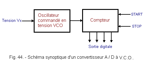
The voltage to be converted Vx is applied to the control input of the oscillator V.C.O. which delivers a rectangular signal whose frequency depends on the voltage Vx. This signal is transmitted to the clock input of a counter which works for a time T determined by the commands on the inputs «Start» and «Stop». At the end of counting and if the time T has been judiciously chosen, the counter indicates a binary number corresponding to input voltage Vx.
A / D converters of this type are slow but very accurate.
3. 7. - COUNTER CONVERTER
These are devices that include a meter, a D / A converter, a comparator, and a control circuit (Figure 45).
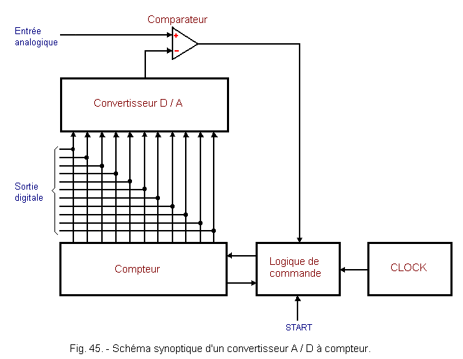
The voltage Vx to be converted is applied to the input «+» of the comparator.
The start of the conversion is given by a pulse on the input «Start» of the control circuit.
At this time, the clock pulses are transmitted to the counter through the control circuit.
The counter will therefore increment each clock pulse.
The binary outputs of the meter are connected to the inputs of a digital / analog converter which delivers an analog voltage in steps. This voltage is applied to the «-» input of the comparator.
When the step voltage, coming from the D / A converter, reaches or exceeds the value Vx, the output of the comparator changes state which informs the control circuit that it must block the counter. At the output of the counter, there is therefore a binary number corresponding to the analog input Vx.
This type of D / A converter is rather slow. In some cases, especially when it is desired to process analog signals varying over time, a down-counter is used instead of a normal counter. This gives a follower converter.
If the output of the D / A converter is lower than the Vx input, the counter counts up and thus the output of the D / A converter increases. If, on the other hand, the same output is higher than the input Vx, the counter counts down, thus reducing the output of the D / A converter.
An example of conversion using a down-counter is shown in Figure 46.
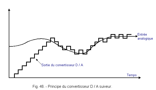
The follower converter is able to react very quickly for small variations of the input signal. For abrupt and large variations, it is as slow as the first-type counter converters.
Thus ends these theoretical lessons devoted to digital electronics and which constitute an excellent preparation to approach the examination of microprocessors and microcomputers.
 Click here for the next lesson or in the summary provided for this purpose Click here for the next lesson or in the summary provided for this purpose |
 Top of page Top of page |
|
Previous Page |
 Next Page Next Page |
Nombre de pages vues, à partir de cette date : le 27 Décembre 2019

Envoyez un courrier électronique à Administrateur Web Société pour toute question ou remarque concernant ce site Web.
Version du site : 10. 4. 12 - Site optimisation 1280 x 1024 pixels - Faculté de Nanterre - Dernière modification : 02 Septembre 2016.
Ce site Web a été Créé le, 14 Mars 1999 et ayant Rénové, en Septembre 2016.