 Converter to Successive Approximations Converter to Successive Approximations |
 Footer Footer |
The Analog / Digital Converter - Converter with Successive Approximations :
3. - ANALOG / DIGITAL CONVERTER
This type of circuit transforms an analog signal into a binary number. As in the D / A converters, the analog values can range from zero to a maximum end-of-scale VA value.
The number of digital combinations is limited by the number of bits available at the output. The analog values between zero and VA are infinite.
In general, it is necessary to use quantization or sampling (cutting) of the input signal.
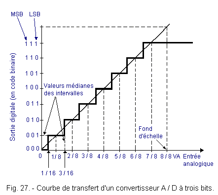
With sampling, the field of variation of the analog signal is divided into more or less regular intervals according to the number of bits available. All analog values between the median value of an interval and the median value of the next interval are translated by the same binary number.
Figure 27 shows the transfer curve of a 3 bits A / D converter.
The binary number 001, for example, corresponds to all the analog values between 1 / 16 and 3 / 16 of VA.
The table in Figure 28 gives the correspondence between the ranges of analog values and the binary numbers obtained at the output of the A / D converter.
| Analog value ranges | Corresponding bit numbers |
| 0 at 1 / 16 | 0 0 0 |
| 1 / 16 at 3 / 16 | 0 0 1 |
| 3 / 16 at 5 / 16 | 0 1 0 |
| 5 / 16 at 7 / 16 | 0 1 1 |
| 7 / 16 at 9 / 16 | 1 0 0 |
| 9 / 16 at 11 / 16 | 1 0 1 |
| 11 / 16 at 13 /16 | 1 1 0 |
| 13 / 16 at 16 / 16 | 1 1 1 |
We can see that the converter is not very accurate. Indeed, the binary number appearing at the output does not make it possible to know with exactitude the analog value which generated it. It only indicates the interval in which the input value is located.
This interval can be reduced by using more bits, but there will always be uncertainty inherent in the conversion process.
There are many types of analog / digital converters ; the most common can be grouped into the following five classes :
parallel,
successive approximation,
ramp,
with voltage-frequency conversion,
to counter.
Each type has its own characteristics, making it more or less capable of solving applications that meet criteria of accuracy, speed, size or cost.
3. 1. - CONVERTER "A / D" IN PARALLEL
It is the simplest converter, it is formed of a series of comparators, as numerous as there are possible intervals minus one.
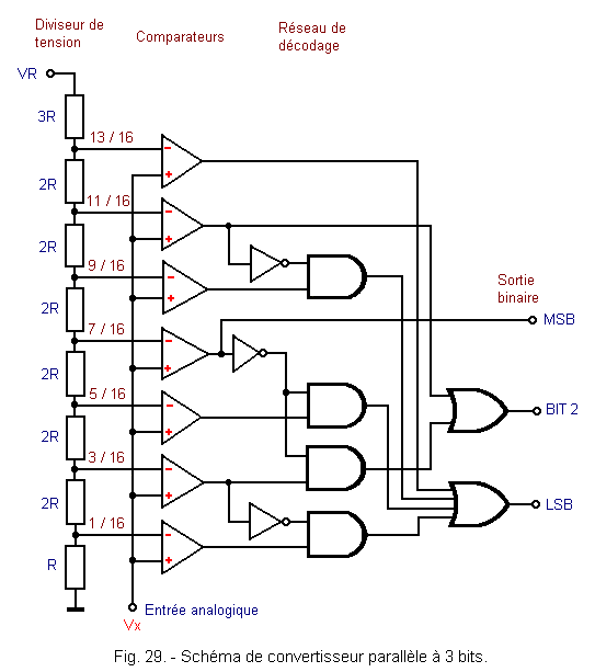
Figure 29 gives the schematic of such a 3 bits converter.
A resistor divider bridge provides the different voltage levels (between 0 and VR) delineating the analog value ranges to be converted. These voltage levels are connected to the «-» inputs of the different operational amplifiers.
The analog input voltage (Vx is applied to all «+» inputs of the operational amplifiers.
Several cases may occur :
![]() The voltage on the «-» terminal is higher than that on the «+».
terminal. The comparator then delivers a negative voltage corresponding to a logic 0.
The voltage on the «-» terminal is higher than that on the «+».
terminal. The comparator then delivers a negative voltage corresponding to a logic 0.
![]() The voltage on the «-»
terminal is lower than on the «+»
; terminal ; in this case, the output becomes positive and corresponds to a logical 1.
The voltage on the «-»
terminal is lower than on the «+»
; terminal ; in this case, the output becomes positive and corresponds to a logical 1.
![]() The two input voltages are identical. The comparator will then issue a logical 0 logique. However, this possibility is almost never considered, because it is very unlikely that the perfect equality of the two tensions is achieved.
The two input voltages are identical. The comparator will then issue a logical 0 logique. However, this possibility is almost never considered, because it is very unlikely that the perfect equality of the two tensions is achieved.
All operational amplifiers make this comparison simultaneously.
If, for example, Vx is equal to 0.3 VR, the output of the first two comparators is 1. This indicates that Vx is greater than 1 / 16 and 3 / 16 VR. On the other hand, the output of the other comparators is at 0 and this indicates that Vx is less than 5 / 16 VR.
On the output of the comparators, we read from top to bottom the binary number 0000011.
In the case where Vx is equal to 0.45 VR, the outputs of the first four comparators are at 1 and the others are at 0, indicating that Vx is greater than 1 / 16, 3 / 16, 5 / 16, 7 / 16 VR is less than 9 / 16 of VR.
On the comparator outputs, the binary number 0001111 is read from top to bottom.
To transform these results into 3 bits binary numbers, a decoding network consisting of logic gates is used (Figure 29).
These converters have the great advantage of being very fast. The binary code follows almost instantaneously the variations of the analog signal, with a minimal delay due to the transit times in the operational amplifiers and in the logic gates.
Unfortunately, the number of elements that compose them grows geometrically with the resolution; indeed, for an n-bit comparator, 2n - 1 comparators are needed.
Thus, for an 8 bits converter, it will require 255 comparators. This results in a very high cost and for this reason, this type of circuit is used only when a high conversion rate is required.
![]() 3. 2. - CONVERTER
WITH SUCCESSIVE APPROXIMATIONS
3. 2. - CONVERTER
WITH SUCCESSIVE APPROXIMATIONS
This is the most used technique, especially when working with computers. This method has the best compromise between speed and resolution.
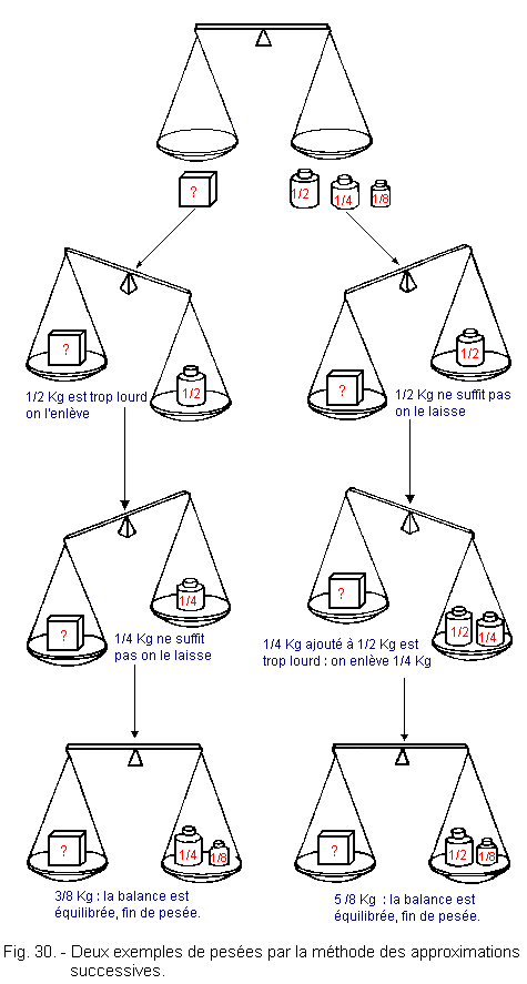
It is a question of determining the value of an unknown voltage Vx, by means of a series of successive «weighings», exactly as one can do with a balance to determine the weight of an object (Figure 30).
We have a series of weights, corresponding to fractions of the range of the scale.
If it is 1 kg, we will have a weight of 1 / 2 kg, a weight of 1 / 4 kg, a weight of 1 / 8 kg and so on.
We then put on a weighing pan, the object to be weighed is on the other, the weight of 1 / 2 kg. If the scale is inclined on the side where the weight of 1 / 2 kg is found, it means that the object weighs less than half a kilogram.
We then replace the weight of 1 / 2 Kg by the weight of 1 / 4 Kg. If now the balance leans on the side of the object, we add the weight of 1 / 8 Kg, and we thus reach the condition balance. In this case, the object weighs of 3 / 8 Kg.
Now consider another case.
After putting a weight of 1 / 2 Kg on a plate and on the other, the object to be weighed, if the scale is inclined towards the object, it means that it weighs more than 1 / 2 kg. So let this weight and we add the weight of 1 / 4 Kg. If at this moment the balance leans on the side of the weights, it is that the object weighs less than of 6 / 8 Kg. We thus replace the weight of 1 / 4 Kg by the weight of 1 / 8 Kg, to obtain the equilibrium. In this second case, the object weighs of 5 / 8 Kg.
For each weight left on the plate, we can associate the binary value 1 and at each unused weight, the value 0. By writing the 0 and 1 following the descending order of the weights, we obtain the binary values corresponding to the weighings of the Figure 30.
The results are 011 for the left weighing and 101 for the right weighing.
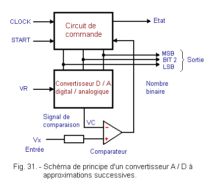
The same principle applies to the analog / digital converter shown in Figure 31.
The circuit is constituted by a digital / analog converter which is associated with a control circuit generating binary numbers.
The analog voltage Vx is applied to the input «+» of the comparator.
The conversion starts when a pulse is applied to the «Start» input.
At the first clock stroke, the control circuit sets the MSB to 1 and all other bits to 0.
The digital / analog converter sees the input bit number 100 and delivers an analog voltage VC corresponding to half of the reference voltage VR.
The operational amplifier performs the comparison between VC and Vx and informs the control circuit.
If Vx is greater than VC, the control circuit leaves the MSB at 1.
If Vx is less than VC, the MSB is brought back to logic level 0.
The control circuit then passes bit N° 2 to state 1. The latter will remain in state 1 if the new comparison voltage VC is greater than Vx or will return to state 0 if VC is less than Vx.
The same process is repeated for bit N° 3 and so on until the last bit (LSB) is processed.
The following example clarifies the mechanism of conversion.
Suppose a voltage Vx = 7.3 volts and a reference voltage VR of 10 volts.
a) The control circuit generates the binary number 100. Since the most significant bit (MSB) has a weight equal to 1 / 2 of VR, the D / A converter delivers a VC analog voltage of 5 volts.
b) The comparator signals that Vx is larger than VC.
c) The control circuit keeps the bit (MSB) in state 1.
d) The control circuit sets bit N° 2 to state 1, thereby producing the bit number 110 which corresponds to the analog voltage VC of 7.5 volts (5 V of the most significant bit plus 2.5 volts of the second bit).
e) The comparator reports that Vx is less than VC.
f) The control circuit resets the second bit to 0.
g) The control circuit sets the least significant bit to 1. The binary number 101 corresponds to the analog VC voltage of 6.25 volts (1 / 2 VR plus 1 / 8 VR).
h) The comparator reports that Vx is greater than VC.
i) The control circuit retains the third bit (LSB) the value of 1.
j) The conversion is complete and we have got the binary number 101.
The Figure 32 shows how the conversion takes place over time. We note that each bit is devoted two equal time intervals.
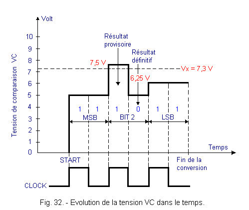
In the first interval (positive window of the clock signal), the control circuit sets a bit to state 1, the D / A converter generates the voltage VC and the comparator informs the control circuit.
In the second interval, the control circuit confirms the state 1 on the bit being processed or decides to reset it to 0.
In the circuit shown in Figure 31, it is noted that the converter has a «state» output.
This is important because during conversion, which is quite slow, the converter delivers incorrect binary signals. It is therefore necessary to know if the conversion is in progress or if it is finished.
It is the role of the «state» output that is at 1 when the conversion is running and at 0 when the conversion is complete.
3. 3. - EVOLUTION OF CONVERTER "A / D" WITH SUCCESSIVE APPROXIMATIONS
The graph in Figure 33 summarizes the pace of the successive approximation conversion as we have just described.
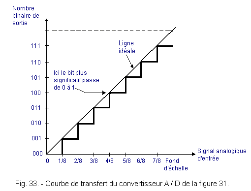
If we compare Figure 33 to Figure 27, there is a clear difference. Indeed, the transfer curve is no longer located on either side of the ideal conversion line, but entirely below. This is due to the fact that the transition from one binary number to another takes place exactly at the right end of each subdivision interval and not at the median value.
For example, the most significant bit (MSB) changes from 0 to exactly 1 at half of the end of scale value (4 / 8 of VR). On the other hand, in Figure 27, the same bit switches for the value 7 / 16 of VR.
The conversion curve of Figure 27 leads to better accuracy. Indeed, in this case, the quantization uncertainty is only 1 / 16 of VR, while in Figure 33, the uncertainty is 1 / 8 of VR. However, it is possible to halve this uncertainty by shifting the transfer curve of the converter upwards.
For this, simply add continuously, a DC voltage of 1 / 16 of VR, to the voltage to be converted Vx.
Figure 34 shows how the approximation improves in the case where the voltage Vx = 7.3 volts.
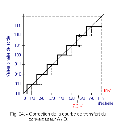
Previously, for Vx = 7.3 volts, we obtained the binary number 101 which is quite far from the ideal curve. After correction, the converter delivers the number 110 which is much closer to the ideal conversion line.
 Click here for the next lesson or in the summary provided for this purpose. Click here for the next lesson or in the summary provided for this purpose. |
|
 Previous Page Previous Page |
 Next Page Next Page |
Nombre de pages vues, à partir de cette date : le 27 Décembre 2019
Envoyez un courrier électronique à Administrateur Web Société pour toute question ou remarque concernant ce site Web.
Version du site : 10. 4. 12 - Site optimisation 1280 x 1024 pixels - Faculté de Nanterre - Dernière modification : 02 Septembre 2016.
Ce site Web a été Créé le, 14 Mars 1999 et ayant Rénové, en Septembre 2016.
