 Digital / Analog to Operational Amplifier Converter
Operational Amplifiers - Digital / Analog to Operational Amplifier Converter :
2. 2. - OPERATIONAL AMPLIFIERS
The graphic symbol of the amplifier is given in Figure 10.
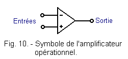
Note that the power supply is not represented. However, on the circuits, it is obligatorily present. Generally, a symmetrical power supply characterized by the presence of three terminals is used : one for the positive voltage, one for the negative voltage, one for the mass.
The ideal operational amplifier has the following characteristics :
![]() Infinite amplifier :
the voltage amplification which is the ratio between the output voltage VS and the input voltage Ve (Figure 11) can be considered practically infinite :
Infinite amplifier :
the voltage amplification which is the ratio between the output voltage VS and the input voltage Ve (Figure 11) can be considered practically infinite : ![]()
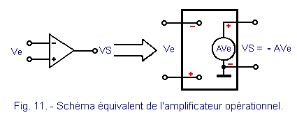
![]() Infinite input impedance : With infinite input impedance, the amplifier does not represent a load for the previous circuit ; in other words, it does not absorb any current.
Infinite input impedance : With infinite input impedance, the amplifier does not represent a load for the previous circuit ; in other words, it does not absorb any current.
![]() Zero output impedance : With an ideal zero output impedance, the operational amplifier can provide all the current required by the load, without influencing the output voltage.
Zero output impedance : With an ideal zero output impedance, the operational amplifier can provide all the current required by the load, without influencing the output voltage.
![]() Zero output voltage for zero input voltage.
Zero output voltage for zero input voltage.
In this case, we say that «Offset» is zero. Offset is an English term, used to indicate the offset of the point of rest from zero.
With the operational amplifier, only an extremely low input voltage is required to bring the output voltage to a very high value, very close to the supply voltage.
In most cases, it is necessary to decrease the gain of the set by adding some components. As an example, we will consider the assembly shown in Figure 12.
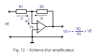
In this circuit, two resistors R1 and R2 were added. R2 provides a feedback between the output and the inverting input of the operational amplifier.
In the ideal amplifier, the input impedance is infinite, so the input current is zero.
The input current Ie also corresponds to the sum of the currents flowing through R1 and R2.
I1 + I2 = Ie = 0
It follows that :
I2 = - I1
The Currents I2 and I1 can also be expressed as follows :
.gif)
As the input current is zero, it can be considered that the voltage Ve across the input impedance is also.
The previous equation becomes :
.gif)
It is therefore deduced that the amplification A of the assembly is equal to the ratio of the resistors R2 and R1 and no longer depends on the amplification of the operational amplifier. The latter has been considered infinite. In reality, it is not, but its value is so high (more than 105) that we can apply the formula VS / VE = - R2 / R1 with peace of mind.
The sign «-» placed before the ratio of the resistors R1 and R2, indicates that the output voltage VS is of opposite sign (or in opposition of phase) with VE.
Another use of the operational amplifier is illustrated in Figure 13.
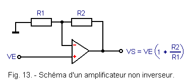
The input voltage VE is applied directly to the + terminal (no inverting input). The reaction network identical to the previous circuit consists of the resistors R1 and R2.
In this type of configuration, the formula that expresses the output voltage is :
![]()
![]() 2. 3. -
DIGITAL / ANALOG CONVERTER WITH OPERATIONAL AMPLIFIER
2. 3. -
DIGITAL / ANALOG CONVERTER WITH OPERATIONAL AMPLIFIER
The principle of a 3 bits digital to analog converter using an operational amplifier is shown in Figure 14.
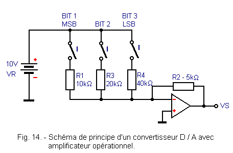
The contacts of the switches can be mechanical or electronic. When the bit is 0, the switch is open, when it takes the value 1, the switch is closed.
Now let's see what happens with a binary number equal to 100. The first contact is closed, the other two are open, as shown in Figure 15.
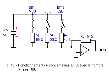
Comparing this figure with Figure 12, we see that the two circuits are equivalent because the two resistors R3 and R4 have no influence.
The output voltage VS is equal to :
It corresponds to half of the input voltage. If only the second switch (number 010) is closed, an output voltage of :
.gif)
In this case, the output voltage corresponds to one quarter of the input voltage.
If finally, we close only the third switch (binary number 001), the output voltage becomes :
.gif)
Either a voltage equal to one-eighth of the input voltage.
To obtain a voltage VS equal to 1 / 16 of the input voltage, a fourth switch and a resistance of 80 kΩ should be used.
If several contacts are closed, the output voltage is obtained by adding the voltages corresponding to each of the switches taken separately.
Thus, for the combination 101, we have :
VS = - (1 / 2 + 1 / 8) x VE = - 5 / 8 x 10V = - 6,25 Volts.
In practice, the circuit as we have just described, is not used. Indeed, if one wanted to work with 12 bits for example, the value of the last resistance would be equal to 20,480 MΩ.
It is quite difficult to achieve resistances of great value with good accuracy.
On the other hand, because of the large differences in values, the variations of the resistances due to the temperature are not identical. The weight of each bit (1 / 2, 1 / 4, 1 / 8, etc.) is no longer accurate and the system accuracy is poor.
2. 4. - RESISTANCE NETWORK (R - 2R)
The solution adopted to overcome the problems created by resistances of too different values is represented in Figure 16.
It consists of using only two resistance values : R and 2R.
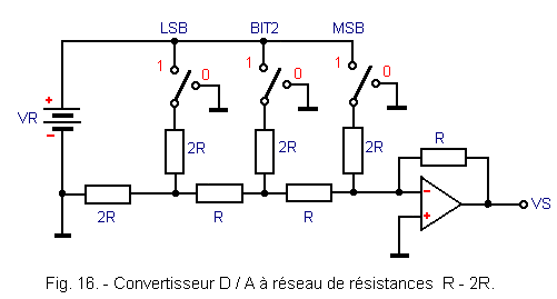
In this circuit, the switches connect the resistors 2R either to the reference voltage VR or to ground, depending on whether the corresponding bit is 1 or 0.
The most significant bit (MSB) is located to the right of the resistor network R - 2R. When the switch corresponding to this bit is in position 1, the output voltage is equal to :
![]()
With the traditional calculations on the voltage divider bridges (which are not carried out here), we prove that the weight of each of the bits is 1 / 2, 1 / 4, 1 / 8, etc ...
If bit 2 is for example 1, the circuit becomes the one indicated in Figure 17.
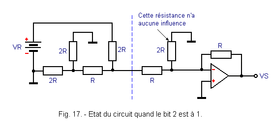
The resistor 2R, corresponding to the MSB bit, has no influence because it is connected between the ground and the input of the operational amplifier which constitutes a virtual ground (potential very close to 0 V).
The resistor network to the left of the dotted line can be summarized as shown in Figure 18-a.
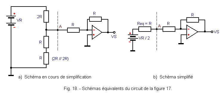
According to Thevenin's theorem, the network situated between the point A and the mass can be replaced by a circuit consisting of a generator in series with an equivalent resistance Req.
![]() The generator has as voltage the value measured at empty between the point A and the mass: here, one obtains VR / 2 since the point A is connected to the middle of the chain of resistors connected to the terminals of the voltage VR.
The generator has as voltage the value measured at empty between the point A and the mass: here, one obtains VR / 2 since the point A is connected to the middle of the chain of resistors connected to the terminals of the voltage VR.
![]() The equivalent resistance Req is equal to the resistance seen between the point A and the mass when the voltage generator VR is replaced by a short circuit.
The equivalent resistance Req is equal to the resistance seen between the point A and the mass when the voltage generator VR is replaced by a short circuit.
Two resistors of 2R in parallel are obtained here, see Req = R.
Finally, the assembly of Figures 17 and 18-a is summarized in that of Figure 18-b.
With the aid of this simplified Figure 18-b, it can be seen that the output voltage is equal to :
![]()
The weight of bit N° 2 is therefore 1 / 4 of VR.
An intermediate solution between the resistor network of Figure 14 and that of Figure 16 is represented in Figure 19.
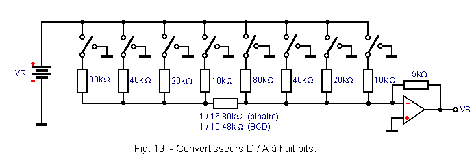
In this circuit, we use two groups of resistors each of which is twice the previous one.
Between the two groups of resistors, a resistor of appropriate value is inserted so as to cause either an attenuation of 1 / 16 if one carries out a conversion in pure binary, or an attenuation of 1 / 10 if one works in code BCD.
2. 5. - "D / A" CONVERTERS WITH INTEGRATED CIRCUITS
D / A converters are currently available as integrated circuits. The converters thus produced achieve an accuracy of the order of 0.05% to 0.0125%.
On the market, there are several types of integrated D / A converters, the simplest is shown in Figure 20.
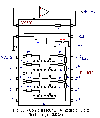
The network of resistors R - 2R and the ten switches which, of course, are realized with field effect transistors are recognized.
Another more complex circuit is shown in Figure 21.
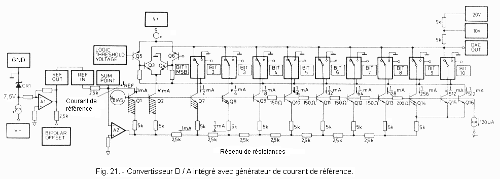
This converter uses a network of resistors R - 2R, each branch of which is powered by a current generator (1 mA, 1 / 2 mA, 1 / 4 mA, 1 / 8 mA, etc ...).
In both cases, the user must add the operational amplifier that is not incorporated in the case. The choice of amplifier will depend on the required switching speed.
The output of the resistor network can be connected to the «-» input or to the «+» input of the amplifier and, depending on the case, a negative or positive voltage is output.
If we use the converter shown in Figure 21, which actually delivers a current I proportional to the input binary number, two different connections can be made (Figures 22-a and 22-b).
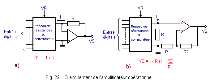
The current I coming from the resistor network depends on the digital signal and the reference voltage VR.
Generally, the configuration of Figure 22-a is preferred because it provides greater accuracy.
![]() 2. 6. - PRECISION OF CONVERTERS
2. 6. - PRECISION OF CONVERTERS
The two main features of a D / A converter are : resolution and accuracy.
As we saw earlier, the resolution depends on the number of input bits that the circuit can process. This number determines in how many steps can be divided the reference voltage VR.
Figure 23 shows the relationship between the digital input and the analog output of an ideal 3 bits converter.
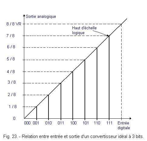
The resolution of this circuit corresponds to the increase of the analog output voltage, caused by the increase of a unit of the input binary number.
In this case, the resolution is 1 / 8 of VR. For a 4 bits circuit, it would be 1 / 16 VR.
Each input bit combination has an output voltage. For example, the binary number 100 determines an output voltage equal to 0.5 VR. In reality, this value is slightly different, it can be 0.49 VR or 0.51 VR. The difference between the ideal value and that actually obtained (± 0.01 VR, that is to say 1% by excess or default) is called the degree of precision or simply precision.
We must not confuse resolution and precision. Indeed, we encounter low resolution converters, for example 3 bits, giving 8 levels, but with very high accuracy. Conversely, there are high resolution circuits (10 to 12 bits of input), but the accuracy is poor.
The factors affecting the accuracy of the converters can be very diverse as we will see now.
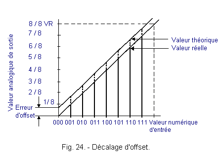
2. 6. 1. - OFFSET NO NULL
When all the input bits are 0, 0 volt should be output. This is not always the case and we are talking about error or offset offset. This difference is constant and exists for all input binary values, as shown in Figure 24.
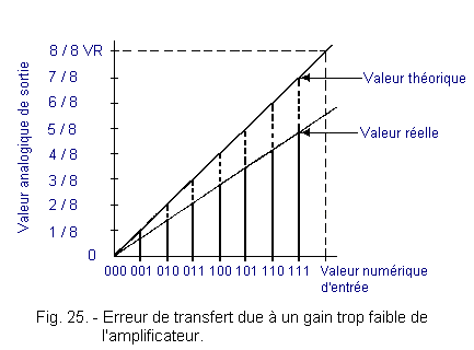
2. 6. 2. - TRANSFER ERROR
This fault occurs when the gain of the amplifier is excessive or too low. Analogue voltage values that are higher or lower than expected are then obtained. Figure 25 shows the difference between the actual values obtained and the ideal values. It is found that the error is even greater than the numerical input value is high.
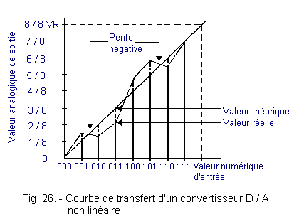
2. 6. 3. - ERROR DUE TO NO LINEARITY
An important cause of inaccuracy is the poor linearity of the system. This is largely due to resistance networks.
The accuracy of a converter depends on the absolute value of each of the resistors and the ratios existing between the various resistances put into service. It is very important that these reports are maintained throughout the field of work.
Figure 26 shows how the transfer curve of a very poor 3 bit D / A converter might look.
It is obvious that such a converter is unusable.
It is inevitable that the value of the resistances varies with the temperature. For this reason, resistance networks integrated in microcircuits are always used ; indeed, with this technology, the resistors are all made of the same material ; moreover, they are very close and therefore undergo the same variations of temperature.
In general terms, the accuracy reveals how much a converter deviates from the theoretical behavior.
Generally, on the manufacturer's notes, one meets two types of precision : absolute precision and relative precision.
The absolute precision is the difference between the analog output that is desired when applying an input binary code, and the output actually obtained.
To correct this difference, one can intervene on the gain of the operational amplifier or on the reference voltage VR.
Relative precision is obtained by relating the deviation to the theoretical value that should be obtained.
 Click here for the next lesson or in the summary provided for this purpose. Click here for the next lesson or in the summary provided for this purpose. |
 Top of page Top of page |
|
Previous Page |
 Next Page Next Page |
Nombre de pages vues, à partir de cette date : le 27 Décembre 2019

Envoyez un courrier électronique à Administrateur Web Société pour toute question ou remarque concernant ce site Web.
Version du site : 10. 4. 12 - Site optimisation 1280 x 1024 pixels - Faculté de Nanterre - Dernière modification : 02 Septembre 2016.
Ce site Web a été Créé le, 14 Mars 1999 et ayant Rénové, en Septembre 2016.