 Evolution of RAM Memories
Evolution of RAM Memory - Dynamic RAM Memory - Volatile and no Volatile Memory :
2. 3. - Timing Diagrams
To operate a memory, certain conditions must be met.
2. 3. 1. - READING IN MEMORY
To read in a memory, it is necessary to present the address of the data which one wants to read, to put the entry of read / write (R / ![]() )
in the active state (generally «1») and to select the memory box by applying an active level on the selection inputs.
)
in the active state (generally «1») and to select the memory box by applying an active level on the selection inputs.
These conditions are described by the timing diagram of Figure 28.
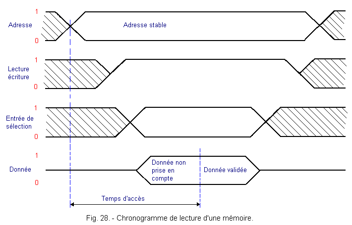
In this timeline and the following, the hatched portions indicate that the state of the entries concerned may vary.
The level of the given output represented halfway between state 1 and state 0 indicates that it is in the «high impedance» state.
The state «high impedance» corresponds to the case where the output circuit is disconnected. This disconnection is carried out thanks to circuits «TRI-STATE» which will be examined in Digital Practice 12.
It is noted that it takes a certain time called access time for the data available at the output to be validated after the address, read / write and selection entries have been activated.
When the selection inputs are activated, the data buses are no longer in the «high impedance» state, but do not give the data corresponding to the desired address.
Indeed, the propagation time of the state of the address and read / write entries is greater than that of the selection entries.
2. 3. 2. - WRITING IN MEMORY
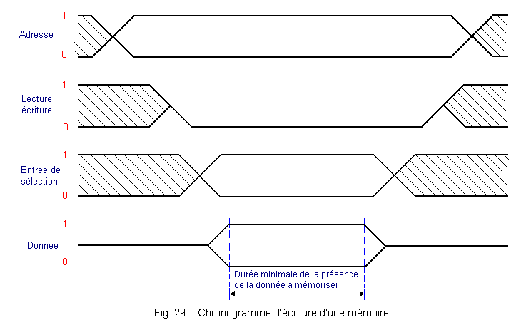
To write to a memory, it is necessary to proceed in a similar way to that used during the reading.
First, we present the address of the data that we want to store, we submit the read / write input to the active state (usually 0), we select the memory box by activating the inputs and finally, the value to be stored on the data buses is applied for a time at least equal to the access time of the memory. These different operations are represented in the timing diagram of Figure 29.
![]() 2. 4. - EVOLUTION
OF RAM MEMORIES
2. 4. - EVOLUTION
OF RAM MEMORIES
In a static RAM memory, each bit of information is stored in a transistor flip-flop which requires at least two transistors. In fact, for this flip-flop to be addressable, the diagram of each memory cell is somewhat complicated and is in the form indicated in Figure 30.
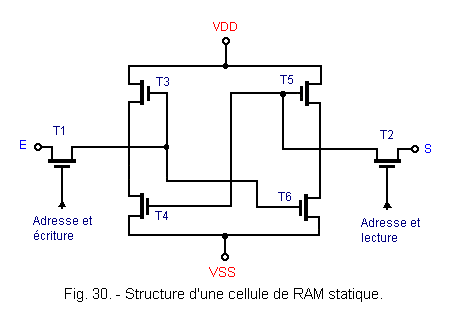
Transistors T3, T4, T5 and T6 form the flip-flop ; the transistor T1 is used to select the memory to write a data, while the transistor T2 is used to select the cell to read its contents.
So not two but six transistors are needed to store a bit. The manufacturers then thought of reducing the number of transistors of a memory cell so as to be able to integrate a larger number on the same surface. They imagined dynamic RAM.
In these, the information is no longer stored as a state of a flip-flop but is stored in a capacitor.
![]() 2. 5. - DYNAMIC RAM MEMORIES
2. 5. - DYNAMIC RAM MEMORIES
Dynamic memories store information (or bits) in the form of electrical charges applied to small integrated capacitors. These capacitors have capacities of the order of 50 femtofarads or 50 x 10-15 farads.
A charged capacitor corresponds to the logic value 1. A discharged capacitor corresponds to the logic value 0. Its charge can be of the order of 500 femtocoulombs, charge corresponding to a voltage of 10 volts at its terminals.
Although this charge value may seem small, it still corresponds to three million electrons and it can be considered that a load a thousand times lower still allow reliable storage.
The diagram of an elementary cell of dynamic RAM is summarized to that represented Figure 31-a.
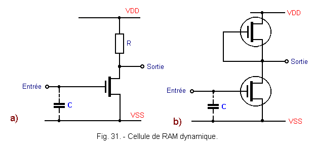
It consists of a MOS transistor and storage capacitor C which is actually the parasitic GRID-SUBSTRATE capacitance of the transistor. The resistor R in series in the drain circuit is actually constituted by a second MOS transistor whose gate and source are connected as shown in Figure 31-b.
A dynamic RAM memory cell therefore actually requires two transistors, three times less than a static RAM cell. This simplicity makes it possible to achieve fairly high integration densities on the restricted surfaces. At present, most vendors offer dynamic 256 kilobit RAM. This reduction in the number of transistors per memory cell reduces the consumption and increases the speed, which constitute two significant advantages.
On the other hand, the major disadvantage of these memories is that if they are dropped after their loading, the capacitors are discharged in a few thousandths of a second and the information is lost.
It is therefore necessary to update the dynamic memories periodically to keep the data as long as the power supply is connected.
Refreshing the memory cells usually takes place every one or two milliseconds, that is 500 or 1 000 times per second. It consists in recharging each capacitor individually before it is completely discharged. Of course, the capacitors which correspond to a logic value 0 and which are initially discharged, must not be loaded during refreshments.
This process requires a periodic signal which can be provided either by a clock generator or by the read signal itself provided that it is repeated regularly.
Thus, in the dynamic memories, there is always a gate used to generate the internal control signals necessary for the regeneration of the data.
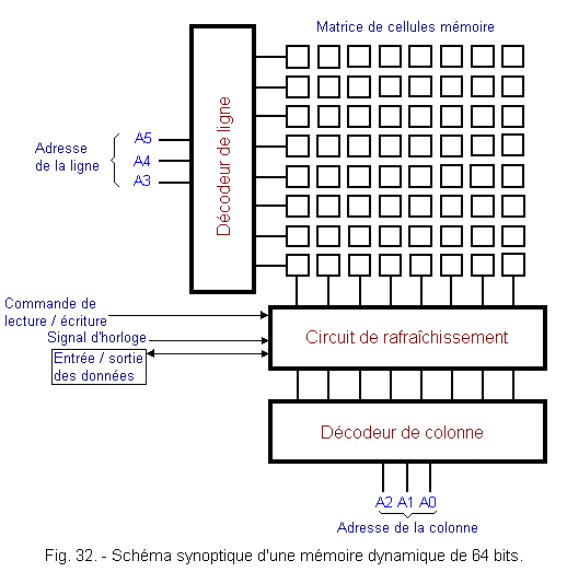
Figure 32 gives the block diagram of a 64 bits dynamic memory.
Let's take a closer look, using Figure 33, the principle of operation of the cooling circuit.
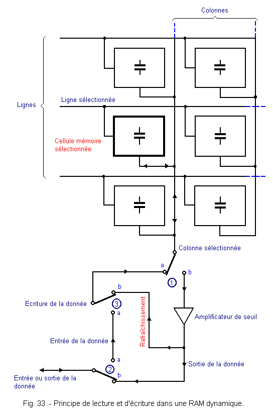
Consider the memory cell selected by the row and the column corresponding to the chosen address (in bold Figure 33). The data passes through the link corresponding to the selected column to which a threshold amplifier is connected.
![]() When it comes to writing in the memory, the inverters
When it comes to writing in the memory, the inverters ![]() ,
,
![]() and
and ![]() are on position «a» and the data arrives at the memory cell, loading the capacitor if it is is a logical 1 and unloading it if it is a logical 0.
are on position «a» and the data arrives at the memory cell, loading the capacitor if it is is a logical 1 and unloading it if it is a logical 0.
![]() When it comes to read the contents of the memory, the inverters
When it comes to read the contents of the memory, the inverters ![]() ,
,
![]() and
and ![]() are on the position «b» and the load of the capacitor of the selected memory cell is applied to the input a threshold amplifier. Depending on the high or low level applied to its input, this amplifier switches to a high or low state and thus delivers the stored bit to the output.
are on the position «b» and the load of the capacitor of the selected memory cell is applied to the input a threshold amplifier. Depending on the high or low level applied to its input, this amplifier switches to a high or low state and thus delivers the stored bit to the output.
Immediately after this reading, the inverter ![]() returns to the position «a» and the high or low state of the output of the amplifier is used to possibly recharge (in the case of the high state) the capacitor of the memory cell.
returns to the position «a» and the high or low state of the output of the amplifier is used to possibly recharge (in the case of the high state) the capacitor of the memory cell.
During a refresh cycle, each cell is read and recharged immediately. To speed up the process, an amplifier is connected to each column and all the columns are refreshed simultaneously : the operation of refreshing a complete memory thus consists in reading sequentially in one or two milliseconds all the lines of the memory.
2. 6. - RAPIDITY OF MEMORIES
We have seen previously that MOS dynamic memories were faster than static memories made with the same technology. Let's see what it means concretely.
A memory is considered more or less fast depending on the longer or shorter time required to read the contents of an address.
More precisely, this speed of the memory is a function of the access time and the reading cycle time.
The access time is the time that elapses between the moment when the memory receives a read command and the moment when it delivers the data contained at the indicated address as output.
The MOS memories have an access time of the order of 100 to 200 nanoseconds, however for bipolar memories, this time is reduced to a few tens of nanoseconds.
The read cycle time is equal to the access time, plus some time required for the memory to prepare to receive the next request.
Indeed, in dynamic memories, when a data has just been read, it must be rewritten immediately to the same address or it will be lost.
This procedure does not exist in static memories that do not lose the contents of an address during playback.
2. 7. - PSEUDO - STATIC MEMORIES
Despite the advantages mentioned above (lower cost, lower power consumption, greater memory capacity), dynamic RAM memories still have the disadvantage of requiring regeneration signals, which complicates the external control circuit.
To remove this defect, some manufacturers have thought to fully incorporate the refresh circuits in the memory box. Thus, seen from the outside, these memories are quite analogous to static RAM memories : they no longer include an input for the clock signal and no longer require any precautionary use concerning the regeneration.
For this reason, these memories are called pseudo-static. This type of housing tends to spread more and more, especially in microprocessor systems. Many memories of high capacity (from 8 kilobytes) called static by the builders are actually pseudo-static type memories.
![]() 2. 8. - VOLATILE AND NO VOLATILE MEMORIES
2. 8. - VOLATILE AND NO VOLATILE MEMORIES
All electronic memories described so far are volatile memories, that is to say, they lose their content as soon as you disconnect the power supply.
When this is restored, the latches constituting the static memories are put in any unpredictable state while the capacitors of the dynamic memories are often discharged although stray pulses can sometimes load them randomly.
In some cases, it is necessary to keep the information contained in the memories even when the supply voltage disappears.
With RAM memory, the only solution is to use a small buffer battery that goes into operation when the main power is turned off.
This is possible with CMOS memories that consume very little. On the other hand, advances in battery capacity mean that small batteries are now able to power CMOS memories of 4 kilobytes for weeks.
The use of this type of battery is quite common in portable devices as well as in industrial systems.
Indeed, in these, an inadvertent interruption of the mains voltage (of a few milliseconds or several hours, as happens from time to time during failures) would otherwise cause an immediate loss of data.
The cost of reloading the memories before restarting the system is such that it is more profitable to pre-emptively add a backup battery.
Nevertheless, this method does not solve all the problems and in many cases, one needs memories containing permanently recorded information.
A simple example is that of the control programs of a pocket calculator which are stored in so-called no volatile permanent memories.
Their contents are introduced once and for all during the manufacturing process.
Unlike RAM that would write and read information, the latter are read-only memories hence their ROM name (Read Only Memory). These ROM will be discussed in Chapter 3.
2. 9. - COMPARISON OF DIFFERENT MEMORY RAM
| Type | Technology | Words from | Capacity in Kbits | Access time in ns | Consumption in mW | Remarks |
| Dynamic RAM | MOS N MOS | 1, 4, 8 bits | 16 at 256 | 100 at 350 | 30 at 40 | These memories must be refreshed every "3 ms" to keep their contents |
| Static RAM | MOS N MOS | 1, 4, 8 bits | 4 at 64 | 150 at 400 | 150 at 600 | Density lower than dynamic RAM. Usually 2 transistors per cell |
| Static RAM | CMOS | 1, 4, 8 bits | 0,256 at 64 | 100 at 600 | 20 at 100 | Low consumption. Can be made no volatile thanks to a battery |
| Static RAM | ECL | 1, 4, 8 bits | 0,256 at 4 | 10 at 45 | 400 at 1 000 | Low access time but capacity (max. 4 Kbits) and high consumption |
| Static RAM | Bipolar TTL | 1 or 4 bits | 64 bits at 4 Kbits | 33 at 50 | 175 at 500 | Each cell is a bistable flip-flop |
2. 10. - EXAMPLE RAM MEMORY
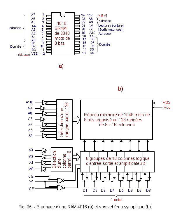
Figure 35-a shows the pinout of a Texas Instruments Type 4016 static RAM memory of 2K words of 1 byte. Figure 35-b shows its block diagram.
 Click here for the next lesson or in the summary provided for this purpose. Click here for the next lesson or in the summary provided for this purpose. |
 Top of page Top of page |
|
Previous Page |
 Next Page Next Page
|
Nombre de pages vues, à partir de cette date : le 27 Décembre 2019

Envoyez un courrier électronique à Administrateur Web Société pour toute question ou remarque concernant ce site Web.
Version du site : 10. 4. 12 - Site optimisation 1280 x 1024 pixels - Faculté de Nanterre - Dernière modification : 02 Septembre 2016.
Ce site Web a été Créé le, 14 Mars 1999 et ayant Rénové, en Septembre 2016.