 Random Access Memories (RAM) Random Access Memories (RAM)
|
Footer |
RAM and Dynamic Electronic Memory :
2. - RAM AND DYNAMIC ELECTRONIC MEMORIES
2. 1. - MEMORY DEVICES
Figure 16 shows a switch used as a memory element. The lever of this switch can be in two different positions : upward or downward.
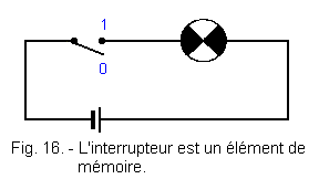
In the first position is associated a lit lamp and at the second the same lamp extinguished. In addition, lever up and lamp lit, we match the logic level 1, while low lever and lamp off, we match the logic level 0. With this convention, the device becomes a memory cell to two states, or binary.
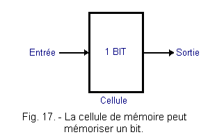
The memory cell, in general, is therefore a circuit or part of a circuit that can store a single bit of information : 0 or 1, as shown in Figure 17.
The flip-flop is the electronic equivalent of the switch we just talked about. Several flip-flops connected in a suitable way, constitute a register, that is to say an electronic memory, not more elementary but able to contain a sequence of bits called sequence.
The bit sequences, stored in the registers, may have a maximum length equal to the number of stages of each register : eight, sixteen, thirty-two bits. These sequences are called words.
The register can therefore be defined as being a memory circuit capable of storing a word.
In previous lessons, you could look at shift registers.
We have seen that there are shift registers with serial or parallel inputs and outputs in series or in parallel.
In Figure 18 is shown the diagram of a register with inputs and outputs in parallel. Often it is not necessary to indicate in detail how the register is designed ; just draw it as a set of adjacent boxes of the same number as the memory cells reserved for each bit.
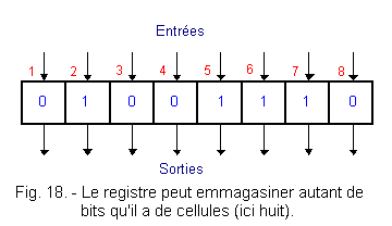
The arrows that represent the flow of bits relative to the inputs and outputs are the same number as the cells.
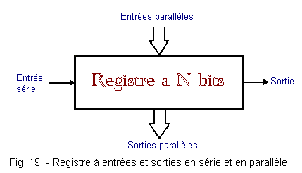
Sometimes, to represent the total flow of bits in and out, in parallel, one uses a large single arrow and the symbol of the register is summarized with only one rectangle.
In this case, the number of memory cells is indicated in number of bits (register of N bits) as you can see in Figure 19.
![]() 2. 2. - RAM MEMORY (RANDOM ACCESS MEMORIES) OR IN FRENCH, MÉMOIRE À ACCÈS ALÉATOIRE
2. 2. - RAM MEMORY (RANDOM ACCESS MEMORIES) OR IN FRENCH, MÉMOIRE À ACCÈS ALÉATOIRE
A RAM is made up of many cells arranged in rows and columns, such as the compartments of a lockbox (Figure 20).
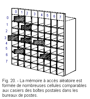
Each cell can be identified using a column number and a row number, just as one does when playing the naval battle.
The term «random access», qualifying this type of memory, means that each memory slot can be accessed without respecting a predetermined order but random needs and choices.
The elementary cell of an electronic memory consists essentially of a flip-flop equipped with an external combinatorial network such that it allows the recording and reading of the data (Figure 21).
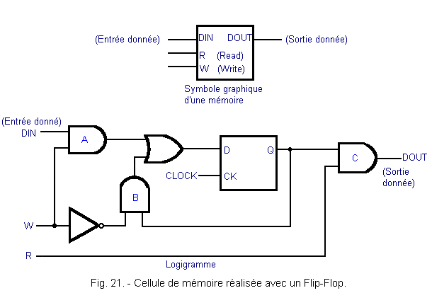
By observing the graphic symbol and the logic diagram, we can see three inputs and one output : one input for the data (DIN), another for predisposing the memory to the writing (W) and a third to predispose it to the reading (R) ; the output is marked with the DOUT symbol. The data 0 or 1 are written in the latch when the input W is high, because thus their passage in memory through the gate A is validated. The symbol W is the initial of «Write» which means to write.
If, on the other hand, the entry W is at the level L, the door A is blocked and the door B passing. In this way, the Q output is connected to the D input of the flip-flop. As a result, each time a clock pulse arrives, the contents of the flip-flop are not lost because it is rewritten through the input D.
The data present on Q is read when the input R is high, which validates the gate C and allows the level available in Q to be displayed on the output DOUT. The letter R is the initial of «Read» which means to read.
The combinatorial gate network that surrounds the flip-flop makes it possible to superimpose the read and write operations even if this is not usually done, because as a general rule, the two operations are performed separately.
In order to differentiate the two operations, an inverter such as that shown in Figure 22 can be used.
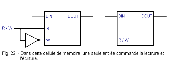
In this way, we obtain a R / W (Read / Write) terminal that will allow writing when it is at 0 and reading when it is at 1.
A single memory cell would be of little interest. It is therefore necessary to put several cells together in order to obtain larger capacities.
We could group them next to each other keeping the separate entrances and exits. Thus, it would be possible to immediately access each cell freely as have the random access memories, but it would also multiply the number of input and output terminals.
In order to reduce the number of legs of the integrated circuit, the elementary memory cell is modified as shown in Figure 23.
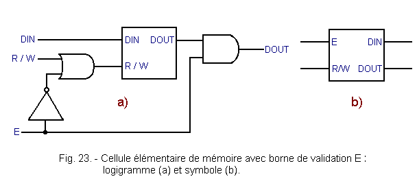
The operation of the new circuit is simple. When E is at level L, the output signal DOUT fails to pass through the AND gate, so you can not read or write because with E at L, the inverter output is at H and the R / W input is at H. The R / W command is used to validate the read or write.
From cells of this type, it is possible to make very large memories. In Figure 24 is shown the diagram of a low capacity memory, four words of two bits.
This means that there are eight bits grouped two by two into four groups and two bits can be read simultaneously.
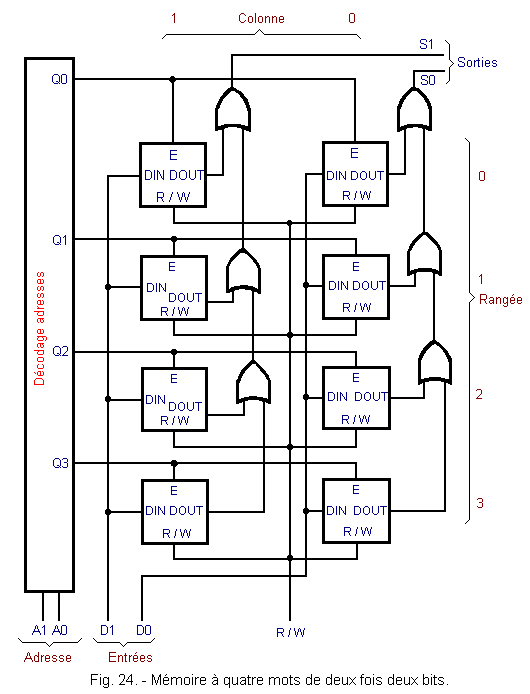
The operation of the assembly is as follows : all the inputs of a column of latches are connected together to one of the two inputs of the memory, D1 or D0, while all their outputs are connected together through successive OR at S1 or S0. Only the latch validated by its input E, can deliver to the input of the OR a 1 which, the OR being in cascade, will appear on the output considered, S0 or S1.
Address inputs A1 and A0 select, by means of a decoder, the row in which to read or write.
When for example A1 and A0 are in the 0 0 state, the Q0 output of the decoder goes high, which validates the two flip-flops of the row 0 by means of the command E.
The term «address» used previously defines the position of the memory box inside thereof ; in our case, the address defines a row where a two bits word is located.
There are memories where the address only defines the position of a single bit ; in this case, it is necessary that the address also indicate the column ; therefore, in addition to the decoder that selects the rows, it is then necessary to have a decoder of columns. In addition, each cell, notwithstanding a validation input for the row, will have a validation input for the column. When both are active, we can read or write.
In Figure 25 is given an example of a memory with 64 cells or bits, each being accessible individually.
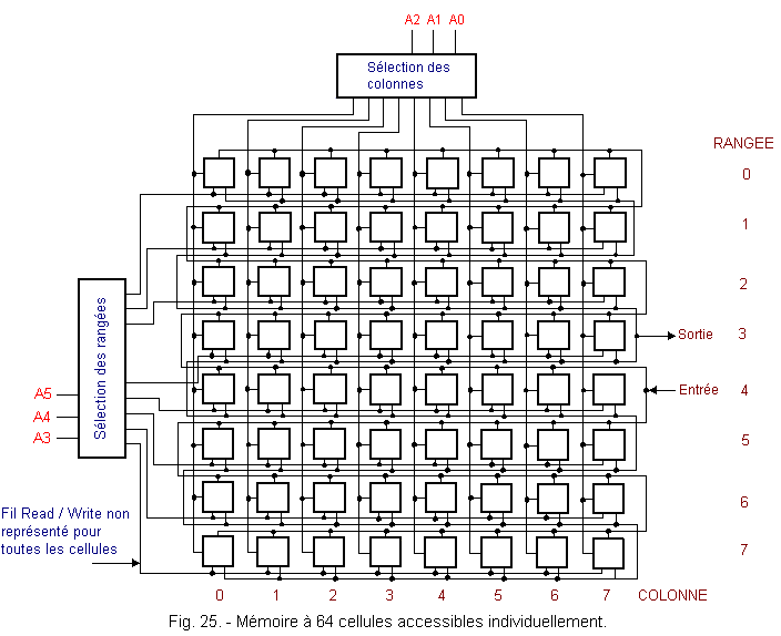
Here, we read or write a single bit at a time. It is therefore necessary to have a six digits address ; indeed, since there are 64 cells, 64 different combinations are necessary and it takes six digits (26 = 64) to obtain this number of combinations.
The first three bits of the address, from A0 to A2, mark the column ; the other three bits from A3 to A5 indicate the row or horizontal line.
The complete address is thus formed as follows :
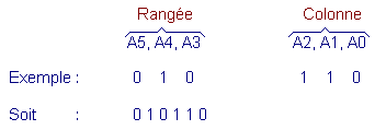
This address designates the cell located on the row 0 1 0 which is the row n° 2 (the third starting from the top) and in the column 1 1 0 that is the column 6 (the seventh starting from the left).
The cells are represented by a small square. For reasons of space, the different inputs and the different outputs are not indicated, however they are shown in Figure 26.
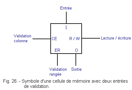
The diagram of the memory of Figure 26, although very simplified, is still quite complex ; we can easily imagine that when the capacity of the memory increases, the complexity of the drawing also increases !
To represent a memory, one therefore uses synoptic schemas even more synthetic, like that of the Figure 27 where all the cells are not represented one by one but replaced by a rectangle (it is about 32 rows and of 32 columns, that is 1 024 cells that would otherwise have to be represented).
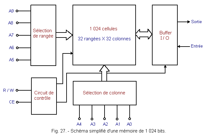
By observing this diagram, we can notice first of all the presence of an additional entry CE, acronym for «Chip Enable» which means «housing selection». This input, as we have seen in some cases, is used when using multiple boxes to make or select a memory or other memory if there were multiple memories in question.
We can then notice the presence of the BUFFER I / O or BUFFER input / output. As we can see, the BUFFER is a tampon circuit, here between the memory cells and the external circuits.
The letters I / O are very important because we meet them very often especially in the microprocessors, they mean INPUT / OUTPUT or Entrée / Sortie.
So far, we have seen different input and output memories, but in practice they are confused to save the pins.
The internal structure of the memories allows it, in fact, these memories are designed so that the input does not disturb the output and vice versa.
 Click here for the next lesson or in the summary provided for this purpose. Click here for the next lesson or in the summary provided for this purpose. |
 Top of page Top of page |
|
Previous Page |
 Next Page Next Page |
Nombre de pages vues, à partir de cette date : le 27 Décembre 2019

Envoyez un courrier électronique à Administrateur Web Société pour toute question ou remarque concernant ce site Web.
Version du site : 10. 4. 12 - Site optimisation 1280 x 1024 pixels - Faculté de Nanterre - Dernière modification : 02 Septembre 2016.
Ce site Web a été Créé le, 14 Mars 1999 et ayant Rénové, en Septembre 2016.