 Example of Memory ROM Example of Memory ROM |
Footer |
Dead "ROM" Memories - ROM Memory Example :
3. - DEAD MEMORIES (ROM)
ROM (Read Only Memories), which means read only memory only, are also known as read only memories. Their main characteristic is to be no volatile.
The elementary cell of a ROM can be obtained from a dynamic memory cell by substituting an open circuit or a ground connection for the capacitor. This results in either state 0 or state 1.
Figure 36 shows a 16 bits read only memory.
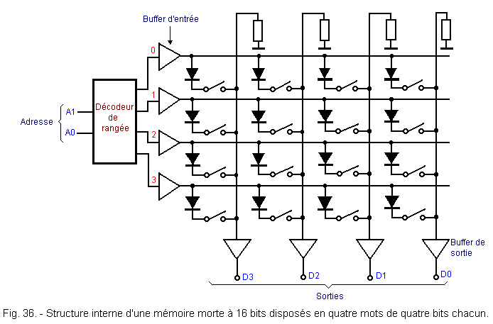
Each memory cell is formed by a diode and a switch that is either open or closed.
A closed switch will therefore electrically contact a row with the column to which it is connected, provided of course that the diode associated with it is passing. This will be conductive if its anode is positive, which requires the presence of a level 1 at the output of the input buffer, level given by the decoder whose output will be 1 (decoder with active outputs at 1) for the decoded address. An example is given in blue Figure 37 for address 112.
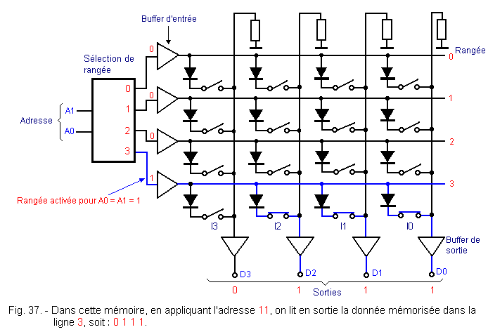
The decoder corresponds to 112 the value 310. The output 3 is therefore 1. Thus, at the output D3 = 0 (switch I3 open), D2 = 1 (switch I2 closed), D1 = 1 (switch I1 closed) and finally D0 = 1 because I0 is closed.
We see that the closed switches for the other rows have no influence because the diodes associated with them are all blocked.
The table of Figure 38 gives the contents of the memory for each of the four addresses (combinations of A0 and A1).
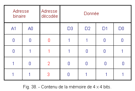
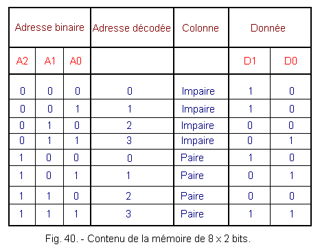
Figure 39 shows the block diagram of an eight bit structured ROM consisting of two bits each, a capacity of sixteen bits.
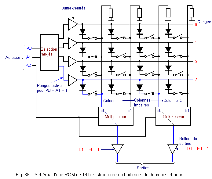
For technological reasons, we keep a square matrix, indeed, it saves on the semiconductor surface necessary for the construction of such an integrated circuit.
The four bits from the four columns are sent two by two on the inputs of two two to one multiplexers. It is therefore possible to output eight two bits words by selecting four rows with either the two and four pair columns, or the odd one and three columns.
To do this, we now use three address bits. The first two bits A0 and A1 make it possible, as before, to select the row, while the third bit A2 makes it possible to choose either the even columns or the odd columns.
Figure 39 gives an example for the address 0 1 1 (A2 = 0, A1 = 1 and A0 = 1). 0112 is decoded as 310 and it is therefore the output 3 of the decoder which is at 1, it then validates the diodes of the third row through the buffer.
The bit A2 is 0, the multiplexer selects columns 1 and 3 (odd columns). We then read D1 = 0 and D0 = 1 : routes in blue color in Figure 39.
The table of Figure 40 gives, according to the possible addresses, and this for Figure 39, the data contained in memory.
The contacts appearing in Figure 39 are not actually mechanical switches but electrical connections internal to the integrated circuit, produced during its manufacture.
The internal arrangement of the electrical connections in question varies at the request of the customer.
To make the circuit according to the specifications of his client, the manufacturer uses a photographic mask on which he adds the desired links.
However, this type of memory can be provided in very large quantities, given the high cost of manufacturing processes using photoengraving and chemical etching.
These circuits come back much cheaper than RAM but the series must have at least a thousand copies.
![]() 3. 1. - EXAMPLE OF MEMORY ROM
3. 1. - EXAMPLE OF MEMORY ROM
You can see Figure 41 the block diagram of a 32K ROM type MCM 68 A332 and its pinout.
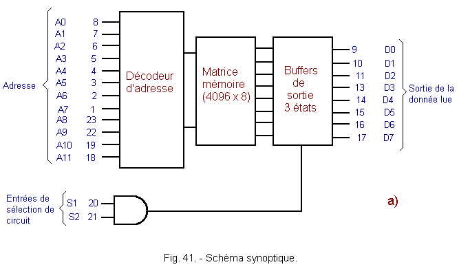
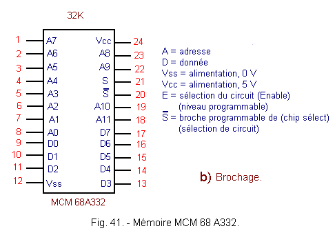
This type of memory includes within the same housing the address decoder and the three-state output buffers.
3. 2. - USE OF ROM MEMORY IN COMBINATION CIRCUITS
Given their properties, ROM memories can, under certain conditions, replace a combinational circuit.
Indeed, if we assimilate an address to a set of input variables, we can consider that the data obtained by reading the memory position at the address in question will be the output variables of the system.
Figure 42 shows the truth table of a circuit.
| a | b | c | S1 | S2 |
| 0 | 0 | 0 | 0 | 0 |
| 0 | 0 | 1 | 1 | 0 |
| 0 | 1 | 0 | 1 | 0 |
| 0 | 1 | 1 | 1 | 0 |
| 1 | 0 | 0 | 1 | 1 |
| 1 | 0 | 1 | 1 | 0 |
| 1 | 1 | 0 | 0 | 1 |
| 1 | 1 | 1 | 1 | 0 |
It will therefore be sufficient to write to a memory 0 0 at the address 0 0 0, 1 0 at the address 0 0 1, 1 0 at the address 0 1 0, 1 0 at the address 0 1 1, 1 1 at the address 1 0 0, 1 0 at the address 1 0 1, 0 1 at the address 1 1 0 and 1 0 at the address 1 1 1 to be able to replace the combinatory circuit with a ROM.
 Click here for the next lesson or in the summary provided for this purpose. Click here for the next lesson or in the summary provided for this purpose. |
 Top of page Top of page |
|
Previous Page |
 Next Page Next Page |
Nombre de pages vues, à partir de cette date : le 27 Décembre 2019

Envoyez un courrier électronique à Administrateur Web Société pour toute question ou remarque concernant ce site Web.
Version du site : 10. 4. 12 - Site optimisation 1280 x 1024 pixels - Faculté de Nanterre - Dernière modification : 02 Septembre 2016.
Ce site Web a été Créé le, 14 Mars 1999 et ayant Rénové, en Septembre 2016.