Explanation of the Operation of the Microprocessor Circuit "Z80" :
4. 3. - OPERATION OF THE Z80 MICROPROCESSOR CIRCUIT
This experiment made it possible to obtain the signatures of the address signals generated by the Z80 ; these are periodic as shown in Figure 21.
Each start of reading of an instruction is made on command of the Z80 by a signal
generated by the microprocessor ; RD comes from the English word READ (lire).
For reasons of space, only the first four address signals have been indicated in Figure 21, relating to the first sixteen addresses among the 65 536 possible. The other signals up to A15, which are not shown in Figure 21, have a similar periodic pattern.
Bit A15 remains low for 32 768 pulses from
and high for the next 32 768 pulses.
The sequence of the bits entering the shift register depends on the address output considered and on the clock signal used. Since in our test circuit it is the signal
which acts as clock, the sequence of A0 and therefore : 01 01 01 01 ... and so on ; that of A1 is on the other hand 00 11 00 11 ... ; that of A2 00 00 11 11 00 00 ... ; that of A3 00 00 00 00 11 11 11 11 ... etc.
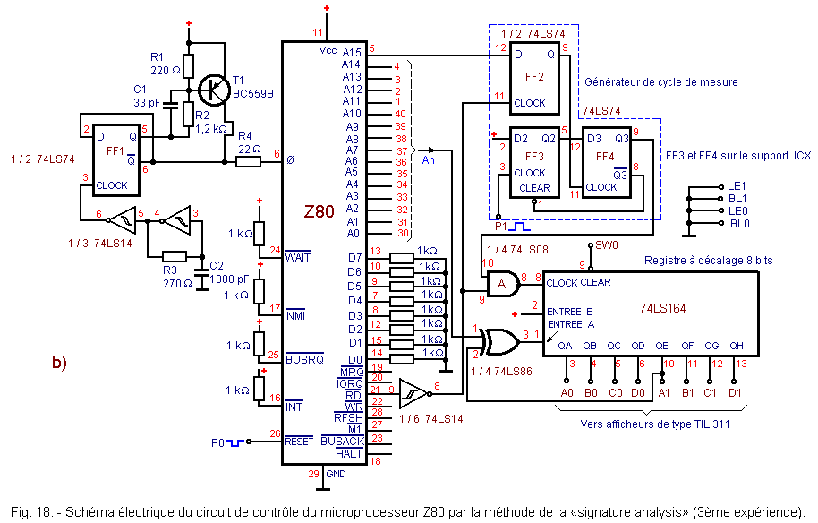
Let us now see in more detail the operation of the circuit which one has just tested, by examining the electric diagram of the Figure 18-b. The part of the circuit drawn to the left of the Z80 is used to generate the clock signal for the microprocessor.
(We postpone here the diagram of the Figure 18-b in order to facilitate the reading of it).
Two Schmitt triggers, connected like the oscillators of the digilab, produce a rectangular signal whose frequency is around 1 MHz. This signal is applied to the clock input of flip-flop 74LS74 whose output, adapted by the transistor T1, makes it possible to control the clock input f
of the Z80.
We already had the opportunity, during practice N° 1, to dwell on the functioning of the adaptation circuit built around T1.
The ,
,
,
inputs are connected to the positive supply voltage via four 1 kΩ resistors so as to ensure the smooth operation of the Z80.
The inputs D0 to D7 are, on the other hand, connected to ground so that the microprocessor always reads the NOP instruction.
The output A15 is connected to the measurement cycle generator which is formed by three D type flip-flops ; that identified by FF2 is used to "smooth" the signal from A15.
Indeed, the address signals generated by the Z80 do not appear exactly as illustrated in Figure 21, because during the time when the Z80 decodes and executes the instruction (here NOP), the seven least significant bits (A0 to A6) of the address bus contain a refresh address for dynamic memories.
In fact, memories of this type lose their content if they are not "refreshed" periodically.
At each cycle, that is to say at each pulse occurring at the output ,
there is incrementation of the refresh address.
Simultaneously, the content of the interrupt register (whose role will be examined later) is presented on the address entries A8 to A15. As a reset (RESET) of the microprocessor is carried out, these bits pass to zero with each pulse of
.
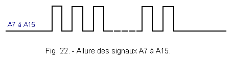
Bit A7 is set to 0 when the contents of the interrupt register and the refresh address are presented on the address bus.
As a result, the signals A7 to A15 have the appearance indicated in Figure 22.
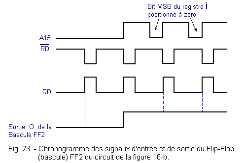
To obtain the signature of the different address outputs, a pulse of duration equal to the period of signal A15 is required.
Since this is forced during each instruction to 0 as shown in Figure 22, it is advisable to format it to obtain a signal similar to those of Figure 21.
For that, it is enough to connect the exit A15 to the entry D of FF2 and to take as clock signal the signal RD obtained by reversing the signal
with the inverter 74LS14.
Thus, the flip-flop FF2 stores the signal present on the input D when the clock RD passes from the low level to the high level, that is to say when
passes to the low level.
Signal A15 is therefore transferred to output Q without the pulses due to the most significant bit (equal to 0) of the interrupt register (I).
This transfer is illustrated by the timing diagram in Figure 23.
The signal A15 thus produced and that obtained by means of the push button P1 in turn control the measurement cycle generator made up of the two flip-flops FF3 and FF4.
These are contained in the integrated circuit 74LS74 inserted on the support ICX.
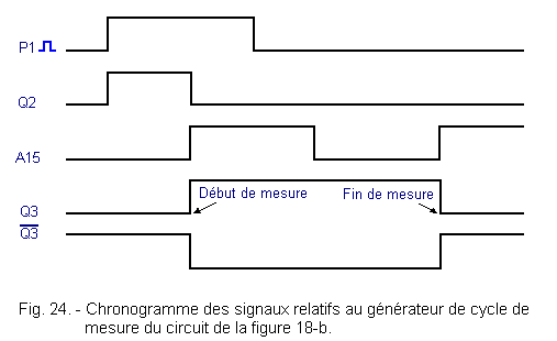
The operation of this generator is simple. Observe Figure 24 : when you press P1, you send a clock pulse to flip-flop FF3 whose input D2 is wired high ; the Q2 output therefore goes high.
The input D3 of the flip-flop FF4, being connected to Q2, is at the high level.
The first rising edge of signal A15 switches FF4 ; thus, the exit Q3 passes to the high level and 3
passes to the low level.
The CLEAR entry of FF3, linked to 3,
is also brought to the low level and therefore resets FF3 to zero ; Q2 goes back to the low level as well as D3.
At the next rising edge of A15, the flip-flop FF4 whose input D3 was at the low level. Q3 then returns to the low level and 3 to the high level. This clears the CLEAR input of FF3 which is ready for another cycle.
As shown in the timing diagram reproduced in Figure 24, a signal is obtained at the output (Q3) of the measurement cycle generator which remains at the high level for a time exactly equal to the period of A15.
It is the time necessary for the microprocessor to generate all the possible addresses from 0000 to FFFF.
The signal Q3 is sent to an input of the AND gate designated by A ; on the other input, the RD signal arrives. The output of this gate is connected to the clock input of the shift register which, in this way, receives the RD pulses only when Q3 is at the high level.
By pressing P1 a second time, another measurement cycle can be started ; in addition, with each new measurement, it is necessary to initialize the register by resetting it to zero, which one obtains by bringing back to entry low the entry
via the switch SW0.
In the previous practice, you got to know the Z80 and the circuits around it better. We can therefore begin to build a more detailed synoptic diagram of the central unit than that presented in Theory 1.(See Figure 3)
We have seen that the Z80 has sixteen outputs for addresses and eight inputs / outputs for data.
The Z80 communicates through these specialized pins with memory and peripherals, for example with the keyboard or the display.
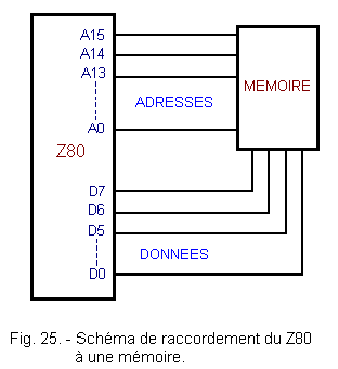
We could directly connect the Z80 to a single memory as shown in Figure 25 but this memory should have a very large capacity.
Indeed, since the address bits are sixteen in number, it is possible to address 65 536 different data (that is to say 64K), each of eight bits, the memory should therefore have a capacity of 65 536 x 8 = 524 288 bits.
Static RAM of this capacity is difficult to find and expensive ; moreover, it is not interesting. Indeed, it is necessary in most cases, to use at least two types of memory : a ROM (or PROM or EPROM) and a RAM.
Read Only Memories (ROM) are used to store the part of the program that should not be changed ; RAM memories, on the other hand, are used to temporarily store the data processed by the microprocessor.
In some cases, RAM is used to write a program during development or testing.
It has already been said that memories are expensive ; therefore, if a capacity of 4K is sufficient for example, it is useless to use a memory of 64K. Thus, on the CPU or UC card, there are in addition to the microprocessor six memory carriers making it possible to insert, in an adequate manner, different types of memory, the addressing being facilitated by straps.
Now you need to know how to distribute these memories and how to connect them to the Z80.
Given that there are six supports for example and that it is possible to address a maximum of 65 536 memory positions, each of these six memories can contain a maximum of 65 536 / 6 = 10 922 data of eight bits each.
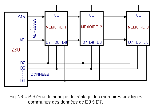
These components therefore have eight inputs / outputs on which the data to be read or written is presented, as shown in Figure 26.
The inputs / outputs of all the memories are connected in parallel with each other and connected to the bus of the Z80.
If the circuit were made as shown in Figure 26, it could not function. In fact, if two or more memories simultaneously transmit data to the Z80, a mixture of these will occur.
It is therefore necessary that only one memory at a time is authorized to operate so that, while data are being sent for example to memory 2, the other memories are disconnected from the circuit.
Similarly, the other memories must not send other data on the same line when the microprocessor reads data from memory 1.
In other words, it is necessary to select a memory, that is to say indicate to which memory the microprocessor wants to access at a given time to read or write data.
For this purpose, each memory box has one or more validation inputs usually designated by CE (initials of Chip Enable) or CS (Chip Select) ; depending on the voltage level applied to these inputs, the component is selected or not.
It is the microprocessor, in our case the Z80, which will have to control the validation inputs.
There are two methods : linear selection and memory decoding.
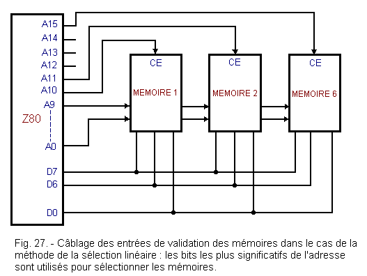
The linear selection method is the simplest and consists of using the most significant bits of the address to select the memories as shown in the diagram in Figure 27.
The Memory 6 is selected when bit A15 is set to 1, memory 5 is selected when bit A14 is set to 1, etc.
The advantage of this method is that it requires no additional circuit. However, it has a major drawback : it is very rigid and does not allow memory to be organized in a flexible enough way, that is to say to arrange the components in the memory spaces (sets of memory positions) better suited.
The resulting memory map (that is to say the arrangement of the memory boxes inside the address field) is absolutely impractical.
In fact, the memory 6 is selected by all the addresses which have the bit A15 equal to 1, that is to say those which go from :
1000 0000 0000 0000
at1111 1111 1111 1111
Half of the possible addresses is therefore reserved for memory 6 which, to be fully exploited, should have a capacity of 32K.
It is therefore better to use the "memory decoding" method. Suppose we want to share the memory so that the last box includes all the addresses which go from :
1 1 1 1
1 0 0 0 0
0 0 0 0 0 0
0
at
1 1 1 1
1 1 1 1 1 1
1 1 1 1 1
1
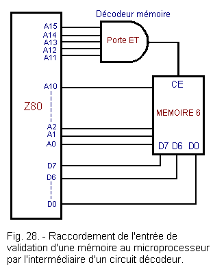
It is therefore a memory of 2K. Note that the five most significant bits (A11 to A15) are always equal to 1 ; by applying these bits to an AND gate, as shown in Figure 28, a signal is obtained which can validate the memory because the output of the AND is only active when the addresses given by the Z80 are included in the interval mentioned above.
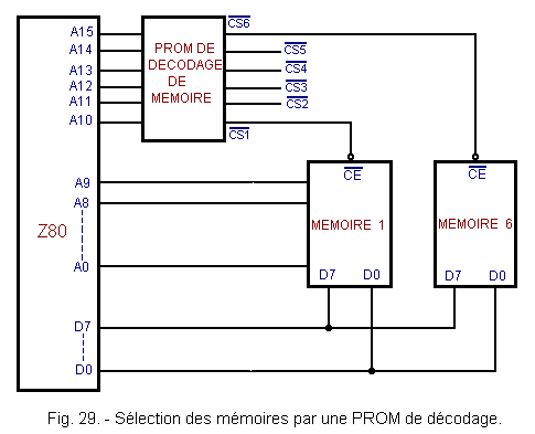
It is possible to use a different decoding network for each memory, but it is even more convenient to use a single decoder for all the memories ; in our case, it consists of the PROM CPU type 74S472 that you tested during Practice 1.
This PROM receives the address bits between A10 and A15 and provides on these six outputs the memory selection signals denoted ,
,
,
and .
The PROM has been programmed so that a selection signal becomes active (low level) when the address sent by the Z80 is located in the address field assigned to the corresponding memory.
Figure 29 shows how the decoding PROM is connected to the Z80 and the memories.
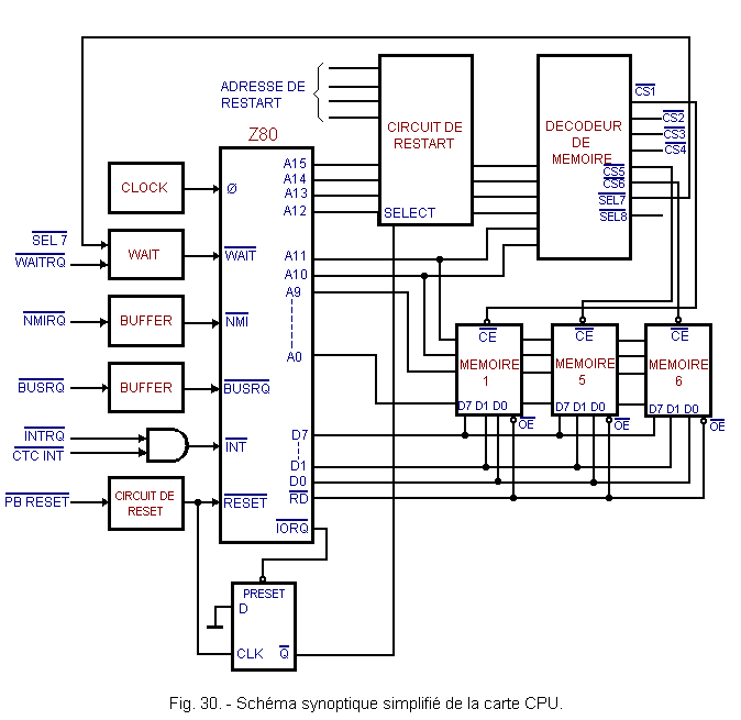
In this practice, you have learned that there is a RESTART circuit (redémarrage).
Thus, the address bits A12, A13, A14 and A15 do not go directly to the decoding PROM, but first pass through the RESTART circuit.
A block diagram of the CPU card including all the circuits that you have seen so far, is drawn Figure 30.
It is noted that the memory decoder provides two other output signals denoted 7
and 8
the first of which is sent to the WAIT circuit.
When we plan to use a slow memory, we program the PROM so that PROM7
is at the low level (active level) each time the Z80 accesses this memory.
Thus, the Z80 remains on standby for the necessary time. The 8
output has another use which will be seen later.
It should also be noted that the memories have another validation input noted
(abbreviated as Output Enable or output validation) and connected to the pin
of the Z80. We have already seen the function of this output : when the Z80 wants to read data from a memory, it sends a low voltage level to the
pin.
In this way, the data output from the memory selected on lines D0 to D7 is validated.
Other entries that can be seen in the diagram in Figure 30 relate to requests and commands from outside the card.
The
command indicates an interrupt request that the Z80 cannot ignore ; when it goes low, the Z80 interrupts the current program to execute the interrupt one.
The
command is on the other hand an interrupt request that the Z80 can ignore ; another interrupt request can come from the CPU card itself, more precisely from a circuit called CTC (initials of Counter Timer Circuit). Under certain conditions, for example at the end of a calculation, it can signal an interrupt request, by activating the entry .
A last command signal is
whose role we will see.
We know that the memories have in common the data bus. It may happen that a device external to the CPU card must use the bus ; in this case, it sends a request to the Z80 via the signal
(abbreviation of Bus Request) and the microprocessor transfers control of the bus as soon as the current instruction is completed.
We will have the opportunity to come back to the function of the different entries, which we have just described briefly.
For the moment, it suffices to know that the addresses and the data travel on lines or buses connecting together numerous devices.
Remember finally that all the signals like ,
are active when they are at low level : this is indicated by the bar.
This practice has enabled you to broaden your knowledge of the CPU card and in particular the operation of the Z80. Obviously, we will not build a microcomputer because it represents a huge and expensive work.


 Conclusion of the Z80 of the CPU Card
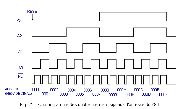
 Click here for the next lesson or in the summary provided.
 Top of page
 Next Page