In this lesson, we will examine the structure and operation of the field effect transistor and then discuss the internal composition of the logic gates according to the different existing technologies.
1. - THE FIELD EFFECT TRANSISTOR
It is customary to designate it by its initials : T.E.C. or F.E.T. (Anglo-Saxon term : Field-Effect-Transistor).
It consists of a uniformly doped semiconductor rod (P or N type) constituting the channel.
On this bar are made two opposite junctions, as shown in Figure 1, of conductivity opposite to that of the channel.
These two zones are electrically interconnected with a common electrode called Gate or Grid.
One end of the channel receives the source name, the other end of the drain.
The channel is weakly doped, while the areas that constitute the grid are strongly doped.
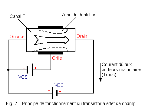
The big difference for this transistor lies in the fact that the gate-source junction is reverse biased (VGS voltage).
The drain-source space receives a bias voltage (VDS voltage).
The operating principle is as follows :
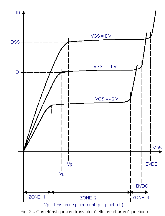
In the absence of gate-source voltage (VGS), the channel leads proportionally with the increase of the VDS voltage.
For a certain value of VDS, the current ceases to grow and becomes constant. This is the pinch voltage or Vp (pinch-off voltage).
The current in the channel is called ID and when it reaches saturation, it becomes IDSS.
If we now apply a voltage VGS to the grid-source space (polarization of the junction in inverse) and that one raises, as previously, the value of ID as a function of VDS, one notes for this current, values more low.
The voltage Vp is reached earlier and corresponds to a current ID lower than IDSS.
This new voltage Vp' is equal to : Vp' = Vp - VGS
As VGS increases, the current ID decreases. From a certain threshold of VGS, the current ID is canceled.
It is generally considered that the current ID becomes equal to zero for :
VGS = Vp.
It is as if the electric field, created by the inverse bias voltage of the gate-source junction, decreases the conduction width of the channel. It is the zone of depletion or impoverishment.
Figure 2 schematizes this phenomenon.
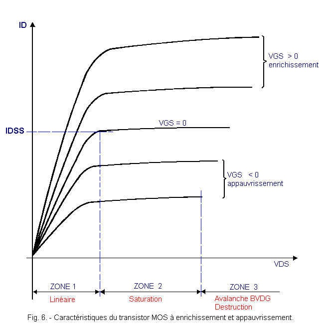
Figure 3 shows the characteristics and important points that relate to the TEC.
The zone
corresponds to the linear part of the characteristic, the current ID grows linearly with VDS (for a given VGS). This zone is used in switching.
The zone
is that of the saturation and is used in amplification.
The zone
is forbidden because it represents the avalanche phenomenon.
The avalanche voltage is denoted BVDG in non-BVDS (BV = break-down voltage, which means breaking voltage or breakdown).
In fact, it is the breakdown of the drain-gate diode. This always occurs for the same voltage difference between the drain and the gate (for a defined type of transistor). This difference is given by the relation :
BVDG = VDS + VGS
When VGS = 0, this voltage BVDG is equal to VDS.
If we keep VDS at the same value and VGS increases (towards negative values), BVDG will decrease. This is what appears on the feature network.
On the other hand, depending on the types of transistors, Vp ranges between 0.5 and 15 volts.
The BVDG voltage varies between 3 and 25 times Vp, always depending on the type of transistor.
It should be noted that the conduction in this type of transistor is almost symmetrical. In Figure 3, we see that all the characteristics pass through the origin and that around it, for weak VDS, the characteristics are prolonged, satisfying the symmetry of conduction (for VDS of opposite signs).
Within certain limits, the changeover between drain and source does not cause any change in the operation.
However, the electrodes are identified by the manufacturer in order to minimize certain capacitive effects, thus making the best use of this device.
These abilities are :
CDS
(between drain and source)
CGS
(between grid and source)
CGD
(between grid and drain)
These are the last two most important ones. By construction, they are attenuated, forcing the user to differentiate the source of the drain.
In the zone of Figure 3 which corresponds to the operation in commutation with VDS < Vp, the transistor reacts as a variable resistor according to VGS.
The minimum value of this resistance is obtained for VGS = 0 (corresponding to the closed switch) and takes the name of Ron (Minimum resistance in the conductive state).
The maximum value is obtained for VGS > Vp (second state of the switch, that is to say open).
R
minimum or Ron: closed switch (VGS = 0)
R
maximum : open switch (VGS > Vp).
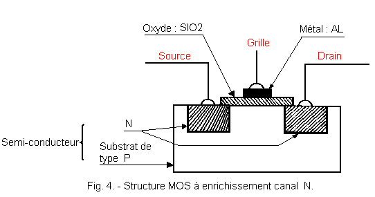
There is another type of field effect transistor which is called MOS transistor (Metal - Oxide - Semiconductor) or MOST (T for transistor).
It is widespread in integrated circuits where it tends to become widespread, at the expense of the bipolar transistor, for reasons of consumption.
Figure 4 shows the structure of such a transistor that differs from the TEC. Indeed, it does not have a junction at the level of the gate, an oxide mask isolates it from the channel, hence the name sometimes given to it : isolated gate voltage.
The operation is as follows :
By applying a positive voltage on the gate, the electrons (minority carriers due to thermal agitation) of the substrate (in the case of Figure 4, this is a material P), are attracted between the zones of material N, constituting the source and the drain. At this point, the concentration of electrons constitutes an enrichment which is translated as an inversion of the conductivity of the substrate thus passing from type P to type N. A current is established between source and drain.
Variations of VGS correspond to variations of ID. In the absence of voltage VGS, the current ID is very low (practically zero).
The substrate is, in general, brought to the most negative voltage, so that the source-substrate and drain-substrate junctions are reverse biased.
This type of MOS is called enrichment (in Anglo-Saxon : enhancement mode).
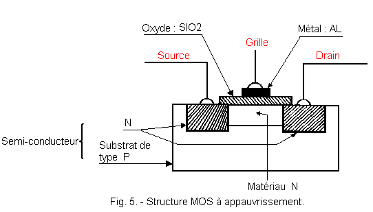
Figure 5 shows the structure of a depletion MOS transistor.
The operation of the latter is different, in the sense that in the absence of voltage VGS, we see a current ID (as for the TEC).
Indeed, the channel consisting of a thin zone of material N located under the gate, is conductive in the absence of voltage VGS. If a negative voltage is applied to the gate, the free electrons of the channel zone will be pushed back by the electric field into the substrate, which results in the reduction of ID. If the voltage VGS is increased, the current ID is canceled.
Here again, it seems that the conductivity of the material is reversed, by impoverishment of the majority carriers.
If, in the absence of voltage VGS, the current ID is maintained at a mean value, by applying to the gate a positive voltage VGS, the electrons of the substrate (minority carriers -----> thermal agitation) will enhance the conductivity of the thin layer of material N and the current ID will become more important.
MOS transistors operating according to the two modes are thus produced with this technique :
enrichment
impoverishment.
This operation is made possible because of the insulating oxide layer separating the gate from the channel.
Figure 6 shows the characteristics of this type of transistor as well as the areas of use.
These transistors have a very high input impedance (due to the isolation of the gate). The resistance in conduction (Ron) is low (a few tens of ohms) and their resistance to the blocked state, very high (several megohms).
These characteristics make it possible, among other things, to use them in logic. The control circuit or input (the gate) is well separated from the output circuit and the two states, blocked or conductive, are very clearly differentiated.
Although the substrate has an obvious action on the conduction of MOS (less than the gate however), it is, in general, internally connected to the housing. It is joined externally, by wiring, at the source.
Its lower consumption than that of the bipolar transistor and its resistance to better voltage are all assets in its favor. On the other hand, it is a little slower. The very high input impedance makes it vulnerable to electrostatic charges, forcing manufacturers to protect its input and users to take extra care in handling. Once the transistor set up on the circuit, there is more risk about it.
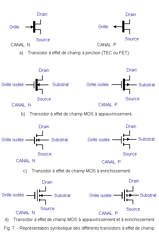
Figure 7 shows the symbols of these different field effect transistors.


 Symbols of different field effect transistors
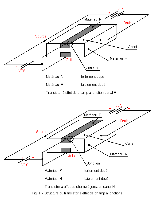
 Click here for the next lesson or in the summary provided for this purpose.
 Top of page
 Next Page