Study of the Bipolar Transistor in Saturated or Blocked Regime :
OPERATION OF BIPOLAR TRANSISTOR IN SATURATED OR BLOCKED REGIME
In the case which concerns us, the transistor is used either in saturated mode, or in regime blocked, that is to say in commutation, in the manner of a switch, copying the two states of this one :
Closed switch = saturated transistor
This state corresponds to the passage of a current in the circuit.
Open switch = blocked transistor
This second state corresponds to the absence of current in the circuit.
The switch is mechanically operated while the transistor is electrically operated.
Figure 16 shows this analogy between switch and transistor used in switching.
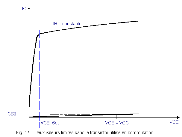
To continue in the way of the analogy between switch and transistor, the latter operating in commutation, two physical quantities are to be taken into consideration. Refer to Figure 17, which shows quadrant 1, which is the output characteristic IC VCE function for given IB.
These two quantities are :VCE
sat. (VCE
saturation) and
ICB0.
VCE
sat. corresponds to the elbow voltage of the characteristic, it is still called waste voltage. This is the minimum value that the VCE
voltage takes for an IC
imposed.
Depending on the current and the type of transistor, this value varies between 0.15 V and 3 V approximately.
ICBO
corresponds to the residual collector current for a zero emitter current. It represents the minimum value of the collector current beyond which we can not go down when the transistor is in the off state. This is the reverse current of the collector-base junction (since it is a reverse junction current, it is due to the minority carriers, therefore, it will increase significantly with an increase in temperature).
The order of magnitude of this current is a few microamperes.
These two limit values correspond to defects. Indeed, saturation, equivalent to the closed switch, a slight tension persists, as if we were in the presence of a contact resistance.
On the other hand, blocking, a slight residual current remains and can be likened to a poorly open switch that has parallel parasitic leak resistance on its contacts.
Another important value is the maximum power that can be dissipated on the collector. It is given by the manufacturer and can be carried on quadrant 1, in the form of a so-called isopower curve.
To highlight the presence or absence of the collector current, or in general, the presence of an electric current, simply place in the circuit a resistor. The voltage appearing at the terminals of this one informs us of this presence and the amplitude of this tension informs us on the importance of this current.
This corresponds to Ohm's law, which we recall :
U = R x I
U : voltage in volt
R :
resistance in ohm
I =
amperage current.
It is a question of determining the resistance R, to be placed in the collector, so as to collect in the output circuit of the transistor a useful signal, which is a function of an input signal.
The determination of this resistance R is influenced by the electrical need of the next current.
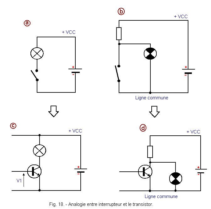
The Figure 18 illustrates two connection possibilities.
In Figure 18-a, the lamp (or load element of the switch) is connected in series with the switch.
When the latter is closed, the current flows and the lamp is on.
When it is open, the lamp goes out.
In Figure 18-b, the lamp and the switch are connected in parallel.
When the switch is closed, the lamp goes out.
When it is open, the lamp is on.
The result of operation is the opposite of that of the previous assembly.
On the other hand, when the switch is closed, if a resistor R is not placed in series, the supply voltage VCC is short-circuited.
In electricity, as in electronics, the short circuit is to be avoided !
It is also necessary to provide a voltage VCC greater than the voltage of the lamp, because for the latter to be on, the voltage VCC must be equal to the operating voltage of the lamp, plus the voltage drop in R.
On the other hand, this arrangement presents an interesting characteristic: the common line of potential.
In the case of combining logic functions with transistors, this allows the design of modules, each representing a basic function and having them end to end, the output signal of one and the input signal of the other having the same electrical reference potential.
The circuit of Figure 18-a will be used preferably at the end of assembly, to power the output member, which will concretize the logic operations performed upstream.
In Figure 18-c, this circuit is the transistor transposition of that of Figure 18-a.
Figure 18-d shows the transistor transposition of the Figure 18-b assembly.
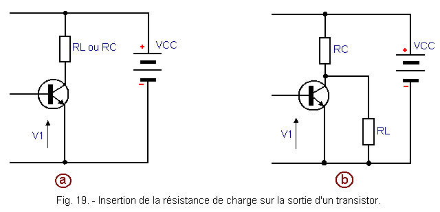
Figure 19 shows the more general cases. It is no longer the lamp, but a load resistance
RL
(L = load = charge).
The collector resistance is identified by RC.
Let's look at what happens in the circuit of Figure 19-a, where the load resistance is merged with that of the collector RC.
In general, it is necessary to start from known data and in this example, it is assumed that we know the voltage required for the operation of the receiver RL
and either its current or its resistance.
This voltage approximately determines the value of the supply voltage VCC
:
VCC
= VRL + VCE
sat.
The voltage VCC
and the current IRL
which becomes current collector, allow the choice of the transistor.
When the transistor is blocked (open switch) the voltage at its terminals VCE
is as follows :
VCE
= VCC - (RL
x ICBO)
It should be remembered that the transistor is not a perfect switch and that in the absence of polarization of the emitter-base junction, circulates in the collector, the reverse current ICBO
of the junction collector-base.
For the drawing of the charge line, the transistor is assumed to be a perfect switch and the voltage becomes :VCE
= VCC
When the transistor is saturated (closed switch), the current flowing through the circuit is given by the relation :
IC
= (VCC - VCESAT) / RL
In the case of the load line, the saturation voltage VCE is neglected (some switching transistors have a voltage drop of less than 1 / 10th of a volt).)
Therefore :
IC
@ VCC
/ RL
Let's put these two values on the quadrant network 1, representing the output characteristic of a transistor which we now know will have to withstand a voltage equal to VCC and a current IRL
= IC.
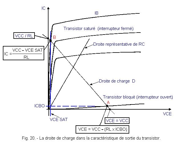
In Figure 20, the line D which connects these two values, is called load line.
The current IC
flowing in RL
when the transistor is saturated corresponds, according to the network, to a base current IB.
We know the relationship :
IC
= bIB
(b = h21E
= current gain)
In the case of Figure 20, this relationship is no longer verified because :
IC
< bIBor
IB > IC
/ b
This relationship verifies that we are saturated. Any variation in IB
no longer results in a variation of IC
in the report b.
In commutation, with no signal at the input, the operating point is at A. With a signal at the input, the operating point changes to B.
The transition from A to B must be made as soon as possible. For now, we will consider that it is done instantly.
The reverse, that is to say the passage from B to A, must be done under the same conditions.
The current IB, determined on the output network, brings us an important element relating to the input signal, that is to say to the output signal of the previous circuit.
Starting from quadrant 4, which represents the inverse transfer characteristic, the value of VBE will be drawn for the VCE SAT in question as a function of the current IB previously found.
We are in possession of the characteristics of the signal V1, which must be applied to the input to obtain the operating point B (that is to say the current IB under the voltage VBE).
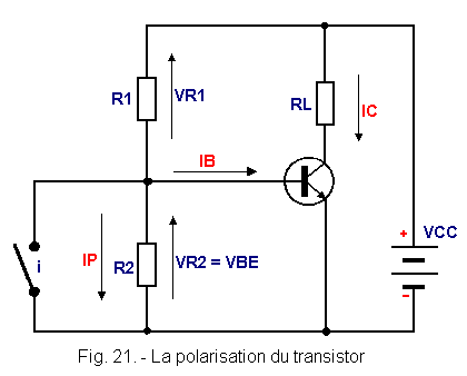
Let us come to Figure 21 in which appear the resistors R1 and R2.
They are mounted as a voltage divider bridge, because the voltage VCC is used to obtain VBE.
In R1, flows the IP current, the divider bridge, plus the base current.
VR1 = R1 x (IP
+ IB)
In R2, the IP bridge current flows, the voltage VR2 is known since it is VBE.
VR2 = VBE
= R2 x IP
For reasons of stability of the operating point, an IP bridge current equal to 10 times the base current IB (difference in IB due to the dispersion of the current gain or to a variation in temperature) is taken.
IP
= 10 IB
Therefore, in R1 flows eleven times the base current and the ohmic value of each of these resistors is as follows :
R1 = (VCC
- VBE) / (11 x IB)
R2 = VBE
/ (10 x IB)
When the switch i is open, the voltage VBE appears across R2, the current IB is injected into the base of the transistor. Current IC flows in RL.
We are on the charging right at point
B.
The transistor is saturated. Practically, the whole voltage VCC is at the terminals of RL, while the voltage VCE is almost zero.
When the switch i is closed, the voltage VBE disappears, the current IB is zero resulting in the cancellation of IC (near ICBO).
We are on the charging right at point A. The transistor is blocked. All the voltage VCC is transferred between collector and emitter of the transistor, the voltage across RL is virtually zero.
the mounting load line that is built considering the transistor as a perfect switch.
the limits on the load line of the switching operation point (blocked or saturated), the transistor being considered as a non-perfect switch.
In this type of assembly, we know that the voltage VCC must be greater than the voltage required by the receiver constituted by RL.
This minimum value of VCC is determined by :
VCC
= VL + (RC
x IL)
It is obvious that we know VL and IL so RL.
The choice of RC allows us with IL to define VCC and possibly to take another value for RC so as not to lead to a voltage VCC too high.
The choice of RC conditions the value of IC considering the transistor as a perfect switch.
IC
= VCC / RC1
Still starting from the same considerations, we can find VCE :
VCE
= VCC - (RC
x IL)2
It should be noted that :
VCC
- (RC x IL)
= VL
The current IC and the voltage VCE allow the choice of the transistor.
This choice being made, we have the output characteristic on which we report the values 1 and 2 that simply connect to get the load line.
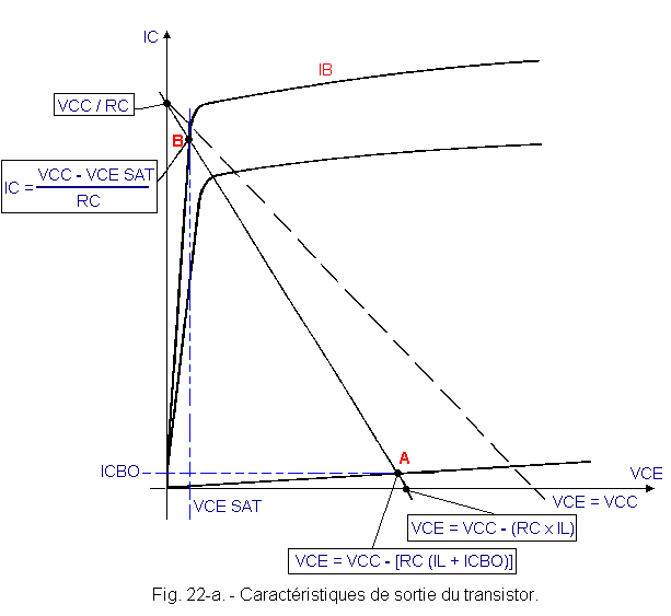
Now, we will look for the limits of operation by not reconsidering the transistor as a perfect switch.
In the saturated state, the current IC becomes :
IC
= (VCC - VCE
SAT) / RC
Considering, under the voltage
VCE
SAT, the current in RLas negligible.
In the off state, the voltage VCE
becomes :
VCE
= VCC - [ (RC
x IL) + (RC
x ICBO) ] = VCC
- RC (IL
+ ICBO)
Figure 22-a illustrates the output characteristic of a transistor on which we have taken these values.
As before, we deduce, from this network, the current IB,
then quadrant 4 the corresponding voltage
VBE
as a function of the VCE
SAT.
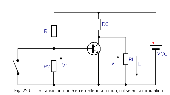
Figure 22-b shows the assembly with its control circuit R1, R2 and i (identical to that of Figure 21).
We know how to calculate R1 and R2 because it is the same reasoning as for the previous editing.
The presence of a base current generates a collector current.
The base current is the consequence of a voltage VBE which polarizes the base-emitter junction in the forward direction.
In this type of assembly, common emitter (Figure 22-b), the output signal is recovered between collector and emitter (voltage VCE).
Between the input and the output, there is inversion of the signal. It is said that the E-C assembly (common emitter) is phase shifter.
In Figure 22-a, the dashed line represents the load line that would be obtained if RL was suppressed.
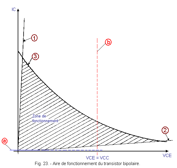
Figure 23 illustrates the operating limits of the transistor.
The line 1 determines, in the saturation zone, the voltage of waste below which, for a given IC, it will not be possible to go down.
The line 2 determines, in the blocking zone, the residual current ICBO below which, for a given VCE, it will not be possible to go down.
Curve 3 informs about the maximum power that the transistor can dissipate.
The lines a and b correspond to the limit values that the load line can take.
a corresponds to infinite RC (infinite ohmic value : cut resistance).
b corresponds to a zero RC (null resistance value : short-circuit resistance). This line can not be reached practically without destroying the transistor or the VCC supply.
We have just skim over the problem concerning the switching transistor (switch operation). The purpose of this lesson is not the study of transistor mounts, but to provide sufficient knowledge to approach the realization of logical processes starting from a material that has its physical limits and, therefore, to split the pitfalls. due to a misinterpretation logic and those due to hazards inherent in technology.
The practical realization of an assembly must always include at least two phases :
a pure and theoretical logical phase
a practical phase involving knowledge of the technology used.
These two steps are equally important.
The second is too often retracted and a lot of setbacks are attributable to it.
The manufacturers make available to the technicians notices relating to the parameters of the circuits they manufacture, it is necessary to take knowledge of them.
The transistor is not only used in switching but also for analog circuits, in the linear zone (amplification), that is to say outside the saturation and blocking zones.
In this respect, in our case, the passage from one zone to another (from point A to point B on the load line) does not take place instantaneously, but with a finite speed, consecutive to certain parasitic capacitances.
This path takes the linear amplification zone which is a disadvantage in switching, and the shorter the transit time, the more we minimize this disadvantage (it results in a degradation of the rising and falling edges of the signal, as well as increased sensitivity, at this time, to external parasites).
This limitation of speed is linked, among other things, to two parasitic capacitances : Cbe and Ccb.
These capabilities are those of the transistor junctions. Cbe is assigned to the base-emitter junction, Ccb to the collector-base junction.
The internal resistance rbb of the base (constituted by the semiconductor zone of the base and the ohmic contact thereof) and the aforementioned capacitors constitute time constants which delay the departure from one point to the other and brake the speed of travel on the right of charge.
The bipolar transistor is used for logical operators in so-called technologies :
RTL :
(resistance logic - transistor)
DTL:
(diode logic - transistor)
TTL: (transistor logic - transistor).
The latter is used for its speed but its consumption and its dissipation do not allow a very thorough integration. So we use another type of transistor, whose operation is a little different and that is called : field effect transistor.
It is the latter that we will examine in the next technology lesson 2.


 Polarization of NPN Transistor
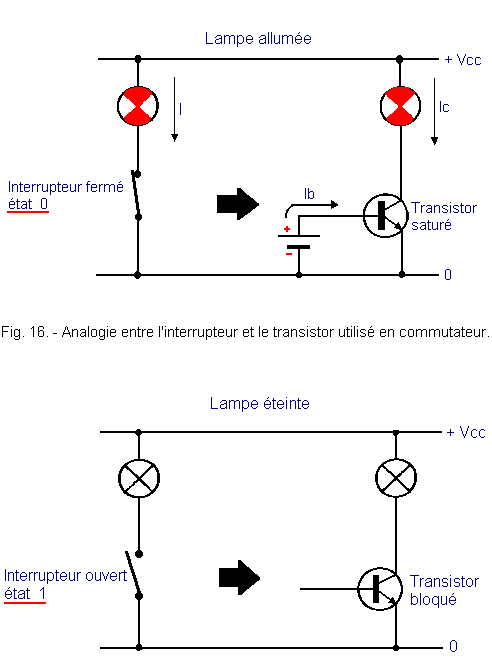
 Click here for the next lesson or in the summary provided for this purpose.
 Top of page
 Next Page