Examination of a CD 4042 Asynchronous Latch Circuit :
4. - FIRST EXPERIENCE : "EXAMINING A LATCH CIRCUIT"
The term "latch" means "verrou, loquet" is used to refer generally to a memory circuit. The D flip-flop used in the previous practice can function as a synchronous latch. It memorizes the logical state present on the input D at the time of the positive transition applied to the CLOCK input.
With the following manipulation, you will check the operation of the integrated circuit CD 4042 containing four asynchronous latch circuits type D. The schematic representation of the quadruple asynchronous latch CD 4042 is shown in Figure 12.
Given the complexity of the circuit, the circuit diagram (as you can see) is simply a rectangle from which the links to the different pins come out. However, each pin is marked with a symbol to understand the operation of the circuit as for the type D rocker you already know.
Indeed, the four pins D1, D2, D3, D4 are as many inputs analogous to the input D (or DATA) of the flip-flop D. The pins Q1, Q2, Q3, Q4 and1,
2,
3,
4
are the complemented outputs of the four circuits latch just as Q and
are the complemented outputs of the flip-flop D. There are then two validation inputs C1 and C2 common to the four flip-flops. These two inputs have a similar function to the input C of the flip-flop R.S.C.
Finally, the pins labeled VDD and VSS must be connected respectively to (+) and (-) of the supply voltage.
4. 1. - REALIZATION OF THE CIRCUIT
a) Make sure that the power supply is disconnected and remove all connections still in place after the last experiment performed in the previous practice.
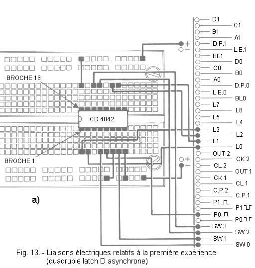
b) Insert the integrated circuit CD 4042 on the matrix, straddling the central groove, in the position indicated in Figure 13-a, paying attention that the 16 pins of the integrated circuit are correctly inserted in the contacts of the matrix.
c) Using the insulated tinned wire you have in your possession, cut pieces of the appropriate length and prepare them in the way you now know and make the connections shown in Figure 13-a.
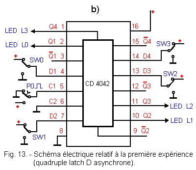
You make the following connections to the input pins of the CD 4042.
input D1 (pin 4) with switch SW0
input D2 (pin 7) with switch SW1
input D3 (pin 13) with switch SW2
input D4 (pin 14) with switch SW3
The outputs Q1, Q2, Q3, Q4 of the integrated circuit are connected to the following four LEDs :
output Q1 (pin 2) with LED L0
output Q2 (pin 10) with LED L1
output Q3 (pin 11) with LED L2
output Q4 (pin 1) with LED L3
The complementary outputs 1,
2,
3,
4
are however not connected : remember that the bar above each symbol of these outputs indicates the presence of an inverted signal relative to the corresponding non-inverted output. So, if for example the output Q1 is at the level L, the output 1
will be at the level H ; it is the same for Q2 and 2,
Q3
and 3,
Q4 and 4.
Input C1 is connected to contact P0
(pin 5) and input C2 to ground "0 V" (pin 6).
The links of the CD 4042 which we have just described are easily controllable in the practical diagram of Figure 13-a as well as in the electrical diagram of Figure 13-b.
In this regard, remember that it is advisable to always consult the wiring diagram to check the accuracy of the connections made in practice.
In this way, as you perform the more complex manipulations planned in the program, you will acquire the ability to easily move from the practical schema to the theoretical schema and vice versa, and especially you will learn to "read" n any electrical logic circuit diagram.
After having made sure that the assembly carried out corresponds to the wiring diagram of Figure 13-b, start the experiment by following the following instructions.
4. 2. - OPERATING TEST
a) Put the four inputs D1, D2, D3, D4 at level L by switching the four switches SW0, SW1, SW2, SW3 to position 0.
b) Power the circuit by connecting the black and red crocodile clips to the 4.5 V battery.
Observe the LEDs, you notice that they are all extinct ; otherwise, unplug the power supply and review the connections made.
c) Now put switch SW0 on position 1 thus applying a level H on the input D1 : you notice that LED L0 lights up.
d) Then put each of the remaining inputs at level H by placing the corresponding switches one after the other at position 1 : you notice that at each input at level H corresponds an output level H indicated by the switching on of the different LED.
With this test, you found that on each output of the integrated circuit in question, you find the level present on the corresponding input. So, if the D1 input is at the H level, the Q1 output will also be at the H level ; if D1 is at the L level, Q1 will also be at the L level. The same situation can be observed for each of the other input-output pairs D2-Q2, D3-Q3 and D4-Q4.
e) Now turn the four switches to any position. For example, set SW0 to position 0, SW1 to position 1, SW2 to position 0 and SW3 to position 1. In these cases, LEDs L1 and L3 light up.
f) Press the P0 button and then switch the four switches as desired while keeping P0 pressed.
By observing the indication of the LEDs, you notice that the outputs do not change state, but that the latter retain the state they had before P0 was activated, which means that the circuit has memorized the situation existing before the action on P0.
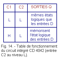
Taking into account the previous observations, it is possible to write the first part of the operating table of the integrated circuit CD 4042 shown in Figure 14, and which summarizes as follows :
With the C1 input at the L level and the C2 input at the L level, the circuit is "transparent" : that is, the outputs reproduce the logical levels of the corresponding inputs.
With input C1 at level H and input C2 at level L, the circuit stores the last logical level present on the input at the instant immediately preceding that when input C1 has passed from level L to level H.
g) Switch off the power supply and bring the C2 input to the H level by disconnecting pin 6 of the CD 4042 from the line connected to the (-) contact and connecting it with another wire of appropriate length to the line connected to the contact (+).
h) Connect the power supply again and repeat the tests previously carried out.
You notice this time that the situation has reversed ; when the input C1 is at the level L, the circuit is insensitive to the changes of levels H and L which are manifested on the inputs. It memorizes the logic level present at the moment when the input C1 passes from the level H to the level L. With the entry C1 at the level H, the circuit is "transparent".
With the help of these last observations, you can complete the operating table of CD 4042 which is therefore as shown in Figure 15.
The operation of the quadruple latch that you have just examined can ultimately be summarized as follows :
the circuit has four inputs and four outputs.
the state of the outputs depends on the state of the two control inputs C1 and C2.
if the C1 input and the C2 input are both H or L, the outputs reproduce or recopy the input status.
if the input C1 is in the state L, when the input C2 goes to the state H, the circuit stores the states of the inputs.
It is the same when the entry C1 is in the state H and that the entry C2 passes to the state L.


 Footer
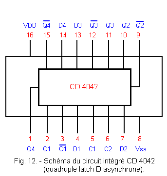
.gif)
 Click here for the next lesson or in the summary provided for this purpose.
 Top of page
 Next Page