Examination of a Parallel-type Summing Circuit and a 2-way Digital Switch :
7. - SIXTH EXPERIMENT : EXAMINATION OF A PARALLEL-TYPE SUMMER CIRCUIT
The serial adder of the previous experiment required eight clock pulses to sum the sum of two eight bits numbers (if the clock pulses required to load both registers) are not taken into account. This summoner is relatively slow.
In this experiment, you will see a much faster method that allows you to add all the bits in parallel.
For this, you will use the integrated circuit MM 74C83 which is a full adder for adding two binary numbers of four bits.
Figure 18-a shows the logic diagram of the summator, while Figure 18-b shows its pinout.
The first number to be added is called A. It is formed by the bits A1 (low weight bit = LSB), A2, A3 and A4 (most significant bit = MSB).
The second number to be added, called B, is formed by bits B1, B2, B3 and B4. At pin 13, the C0 restraint from a possible previous sum is applied.
The result of the sum of the numbers A and B is formed by the bits S1, S2, S3 and S4.
The output C4 of the pin 14 is the retention of the sum made. It can be connected to the input C0 of a possible next adder to add numbers of more than four bits.
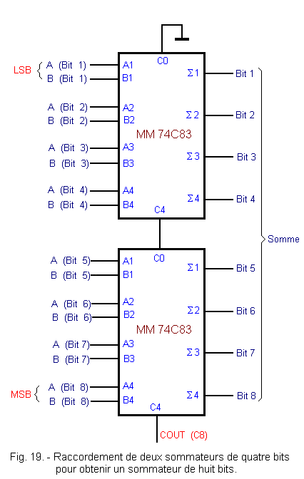
Figure 19 shows how to connect the two four bits summers to add two eight bits numbers A and B.
7. 1. - REALIZATION OF THE CIRCUIT
a) Remove all integrated circuits and links from the previous experiment from the matrix and ICX support.
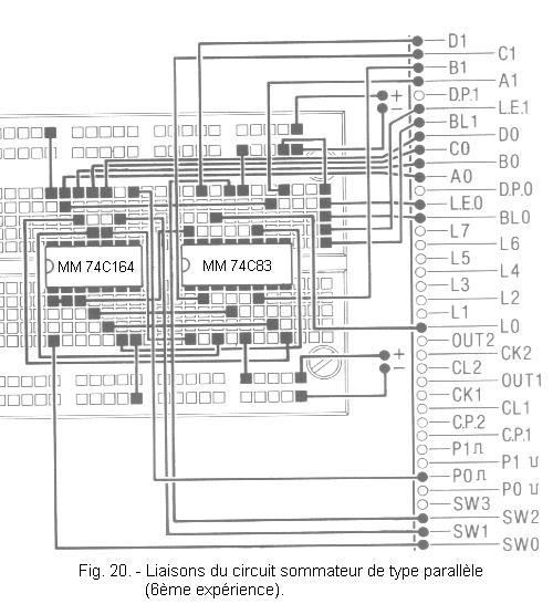
b) Insert on the matrix the integrated circuit MM 74C83 (complete summator) and the integrated circuit MM 74C164 (shift register having eight parallel outputs) in the positions indicated in Figure 20, then make the corresponding connections.
The electrical diagram of the circuit that you have just made is given in Figure 21-a, while Figure 21-b shows the corresponding block diagram.
The circuit consists of a register where we load the two numbers to add A and B and a parallel summator. The register can be reset by means of the switch SW1 by switching the latter to the position 0. The clock signal is provided by P0. The data is entered by pressing SW0.
The result of the sum is visualized by the display DIS1, while the term A is visualized by the DIS0 display ; the restraint is visualized by LED L0.
7. 2. - OPERATING TESTS
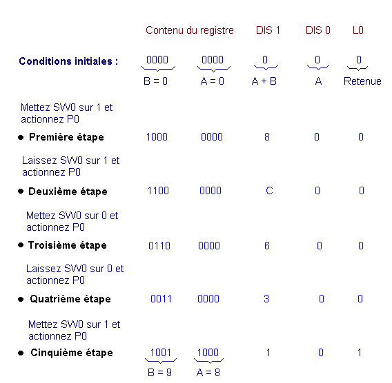
It is a question of adding two numbers of four bits. By way of example, we will add 1001 and 0011, that is to say in decimal code 9 and 3.
For that, we will load the register with these two numbers.
As soon as the loading is carried out, the result of the sum is indicated by the display DIS1. The time taken by the summator to perform the addition is of the order of 125 ns.
a) Put SW1 and SW2 on the 0 position.
b) Switch on the Digilab : both displays show 00 and the LED L0 is off. Indeed, with SW1 on 0, the register is set to zero by means of the entry CLEAR.
c) Set SW1 to position 1 : the CLEAR input is disabled.
d) Following the same procedure as the previous experiment, you will now load the register with SW0 and P0 acting as clock.
The different steps of the procedure are listed below.
We go from one state to another using a clock pulse generated by the push-button P0.
You observe that at this moment the LED L0 is lit, which means that there is a restraint.
Indeed, as the register loads, the summator performs the addition of numbers on its inputs.
In the fifth step, A is 8 and B is 9 ; the sum 8 + 9 = 17 gives in hexadecimal 1116. There is therefore a restraint which is indicated by L0.
There is still a restraint :
indeed, A + B = C + 4 = 1016.
This results in the result : C, which appears on DIS 1 equivalent to 12 in decimal code.
If now we want to add a unit to the result, the new result must be D. Indeed :
C + 1 = D
in hexadecimal code
The method is very simple : it suffices to supply 1 to the summing input of the summator, that is to say C0.
e) Put SW2 on position 1 : you read D on the display DIS 1.
f) With the tests completed, turn off the Digilab.
In summary, this experiment has allowed you to see that a parallel type adder immediately makes the sum of the numbers that appear on the inputs.
During the experiment, you could see many examples of sums before reaching the final result.
For example, in the first step you saw : 0 + 8 = 8
to the second : 0 + C = C
and so on until the seventh step : 6 + 2 = 8
and at the eighth : 3 + 9 = C
You have also seen examples of overflow as in the sixth step with : C + 4 = 1016
The procedure required the serial loading of the register and therefore it was not until the two numbers were loaded before reading the final sum.
If the terms had already been present in the register, the sum would have required only the propagation time of the adder (of the order of 125 ns).
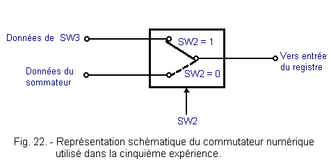
In the fifth experiment, four NOR gates were used to form a circuit providing the switch function. Thus, one could send to the input of the register MM 74C164 one or the other of the two signals applied to the inputs of the switch according to the state of SW2.
A schematic representation of this circuit is given in Figure 22.
This is equivalent to a mechanical switch which inputs to the input of the register the data relating to SW3 when SW2 is at position 1 or the data from the summator when SW2 is at position 0.
In the following experiment, you will examine in detail an equivalent circuit at any point made with NAND gates instead of NOR gates.
8. 1. - REALIZATION OF THE CIRCUIT
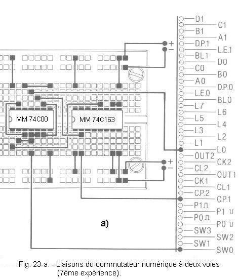
a) Remove from the matrix the integrated circuits in the previous experiment as well as the related links.
b) Insert on the matrix the integrated circuits MM 74C163 (modulo counter 16) and MM 74C00 (quadruple NAND) in the positions indicated in Figure 23-a and make the corresponding connections.
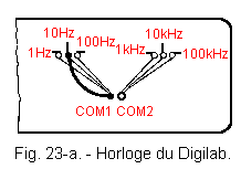
c) Arrange the first Digilab clock generator on the 10 Hz frequency.
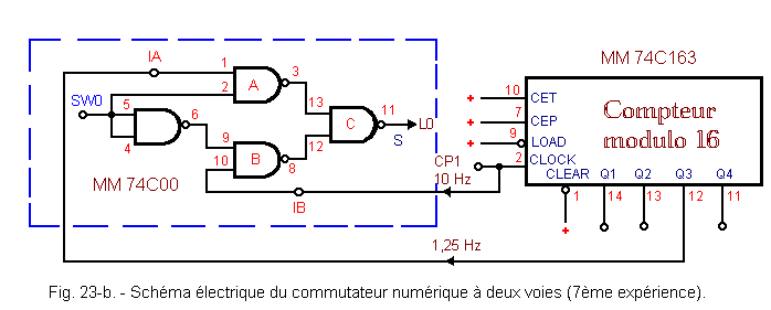
The electrical diagram of the realized circuit is given in Figure 23-b.
The counter MM 74C163 functions here as divider.
The 10 Hz rectangular signal from CP1 is divided four times in succession by two. Thus, a 5 Hz signal is obtained at the Q1 output, a 2.5 Hz signal at the Q2 output, a 1.25 Hz signal at the Q3 output and a 0.625 Hz signal at the Q4 output.
The 10 Hz and the 1.25 Hz signals are sent to the NAND four doors network.
8. 2. - OPERATING TESTS
a) Put SW0 on the 0 position.
b) Turn on the Digilab.
c) Observe L0 : it should flash at the frequency of 10 Hz.
d) Switch SW0 to position 1.
e) Observe L0 : it should flash at a frequency of 1.25 Hz.
f) Switch SW0 alternately on 0 and on 1 : you notice that SW0 controls the switch so as to send to LED L0 either the 10 Hz signal or the 1.25 Hz signal.
g) Turn off the Digilab.
The circuit you just experimented with is the simplest type of digital switch. It is widely used to send on one driver one of two signals depending on the level of a control input. Here, the switch SW0 plays the role of the control input.
The operation of the switch is simple : when SW0 is at the level H, the gate A is validated and the signal of 1,25 Hz is thus found at the exit S ; door B is disabled.
On the other hand, when SW0 is at the level L, the door B is validated and the door A is invalidated ; it is therefore the signal of 10 Hz which is found at the output S.
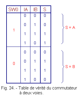
The truth table of the circuit is shown in Figure 24. The two inputs of the switch are called IA and IB.


 Review of a 2-Way Digital Switch
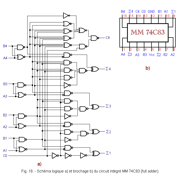
.gif)
.gif)
.gif)
 Click here for the next lesson or in the summary provided for this purpose.
 Top of page
 Next Page