To add two numbers of more than 1 bit, two methods can be used : the sum in series and the sum in parallel.
With the first method, a single summator is enough while with the second, it takes as many summers as there are bits.
In this experiment, you will see an example of a sum in series in which the bits are added one after the other. Two shift registers are used for this purpose.
6. 1. - REALIZATION OF THE CIRCUIT
a) Leave the integrated circuits of the previous experiment on the matrix and remove the dotted links shown in Figure 10.
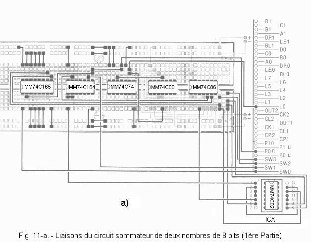
b) Insert the integrated circuits MM 74C74 (double synchronous D-flip-flop), MM 74C164 (serial-parallel 8-bit offset register) and MM 74C165 (parallel-series 8-bit offset register) into the matrix in the positions shown in Figure 11-a.
c) Insert the integrated circuit MM 74C02 (Quad NOR) on the ICX socket.
d) Make the links shown in black characters in Figure 11-a and Figure 11-b. carefully while looking at the theoretical diagram in Figure 12-a.
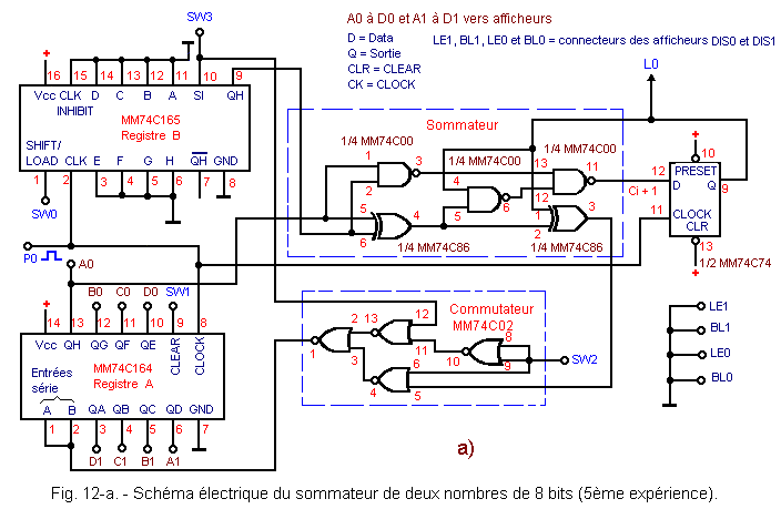
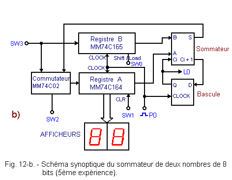
The electrical diagram and block diagram of this arrangement are reported respectively in Figures 12-a and 12-b.
You notice that the circuit consists of two shift registers A and B, both of which can be loaded in series.
The entry of the register A can be connected through the switch formed by the four NOR gates, either to SW3, or to the output S of the summator.
This switch is controlled by switch SW2.
The input of the register B is connected to the switch SW3.
The serial outputs of the registers are connected to the inputs of the summator. A D flip-flop memorizes the hold of a sum for the next sum.
The contents of register A are visualized thanks to the two displays.
6. 2. - OPERATING TESTS
a) Switch the four switches as follows :
SW0, SW1 and SW2 on the 0 position.
SW3 on any position.
b) Switch on the Digilab : you will notice that both displays indicate 00. In fact, the SW1 switch connected to the CLEAR input of the MM 74C164 forces it to state 0. The LED L0 will be on or off according to the state that the scale will take when powering up.
Suppose we want to make the following sum :
181 + 53
(in decimal code)
which gives in binary :
10110101 + 00110101
and in hexadecimal code :
B5 + 35
The procedure to follow is the following :
The register A (MM 74C164) is loaded with the number 18110.
The register B (MM 74C165) is loaded with the number 5310.
The sum is done bit by bit, shifting the contents of the registers to the right.
Thus, a single number is presented at the entry of the summator at a time. The intermediate hold is stored by the D flip-flop. The result of the sum is loaded into the register A and can be read at the end of operation on both displays.
6. 2. 1. - LOADING REGISTER A (MM 74C164)
The register A can be loaded in series with the data coming from the output of the switch. This data can be either the result of the sum coming from the output S of the summator (pin 3 of the MM 74C86), or the logical state imposed by the switch SW3. This choice is made via the switch SW2.
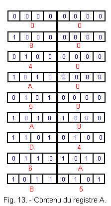
we will now load the number 18110, that is 10110101 in binary.
Make sure that SW0 is in the 0 position so that the serial input Serial Input (SI) of register B is inhibited and do the following :
a) Switch SW1 to position 1 so the CLEAR input of the register is no longer activated.
b) Switch SW2 to position 1 : thus, at each clock pulse delivered by P0, the register loads with the logic level provided by SW3.
c) Set SW3 to 1 and press P0 : the displays show 80.
d) Set SW3 to 0 and press P0 : the displays show 40.
e) Set SW3 to 1 and press P0 : the displays show A0.
f) Set SW3 to 0 and press P0 : the displays show 50.
g) Set SW3 to 1 and press P0 : the displays show A8.
h) Set SW3 to 1 and press P0 : the displays show D4.
i) Set SW3 to 0 and press P0 : the displays show 6A.
j) Set SW3 to 1 and press P0 : the displays show B5.
The Figure 13 shows the contents of the register A after each clock pulse and the corresponding figure in hexadecimal that can be read on the displays.
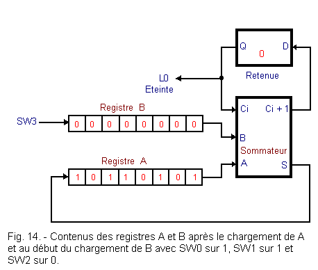
6. 2. 2. - LOADING REGISTER B (MM 74C165)
Switch SW0 is in position 0, register B is loaded with the levels present on the parallel inputs A, B, C, D, E, F, G and H.
In our case, these entries being all connected to the mass, the contents of the register is thus 0.
By setting SW0 to position 1, the register is in SHIFT mode and the serial input SI connected to SW3 is enabled.
The offset of the contents of the register B is done in the same way as that of the register A. However, there is a disadvantage : the clock signal being common to the two registers, while the contents of the register B are shifted, that of the register is also.
To prevent the contents of register A from being lost, SW2 must be set to 0. Thus, the input of register A is connected to the output S of the summator.
At each clock pulse, the result of the sum made by the summator is stored in the first stage of the register A.
This sum does not alter the contents of the register A. Indeed, the output QH of the register A is connected to the input A of the summator, while the input B of the latter receives the contents of the register B which is 0.
Thus, S = A + 0 = A.
The register A is thus looped back on itself. This is highlighted in Figure 14.
a) Make sure that SW1 is in position 1 in order to make CLEAR entry inactive and thus validate register A.
b) Put SW0 on position 1 : you thus validate the serial entry of the register B which is ready to work in mode SHIFT.
c) Put SW2 on position 0 : the input of register A is connected to the output of the summator. The displays show B5.
d) Leave SW3 on 1 and press P0 : the displays show DA.
e) Set SW3 to 0 and press P0 : the displays show 6D.
f) Set SW3 to 1 and press P0 : the displays show B6.
g) Set SW3 to 0 and press P0 : the displays show 5B.
h) Set SW3 to 1 and press P0 : the displays show AD.
i) Set SW3 to 1 and press P0 : the displays show D6.
j) Set SW3 to 0 and press P0 : the displays show 6B.
k) Set SW3 to 0 and press P0 : the displays show B5.
At the end of this loading, the displays indicate B5 and thus confirm that the register A has not lost its initial content.
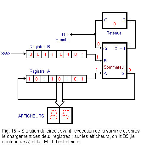
6. 2. 3. - EXECUTION OF THE SUM
At this stage of the experiment, the two registers are loaded with the two numbers whose sum is to be known.
Figure 15 schematically illustrates the circuit situation.
As you can see, the first two bits (LSB) to be added are present on the inputs of the summator. At the exit, we already find the sum which is 0 and the restraint which is 1.
It is now a question of storing this first result by proceeding as follows :
a) Operate P0 : the sum coming from the output S is loaded in the first stage of the register A, while in the register B enters the data relative to the state of the switch SW3 (this data does not have any importance for the sum of the two binary numbers).
The contents of the two registers are shifted one position to the right, which gives the situation illustrated in Figure 16.
b) Operate P0 seven times in a row ; after each partial sum, the contents of the registers are shown in Figures 17-a and 17-b where the displays and the LED L0 are also indicated.
After the eighth clock pulse, you can read on the displays the result of the sum, that is EA (in hexadecimal).
c) After the experiment is complete, turn off the Digilab.
Let's check now if the result of the sum is correct.
The sum to be made was :
181 + 53
= 234 in decimal code
The found result is
EA16; if we translate in decimal code, we get :
EA16
= E x 16 + A = 14 x 16 + 10 = 224 + 10 = 23410.
The state of the LED L0 was ignored since it was off.
If we had made the following sum :
250 + 240
(in decimal) or 1111 1010 + 1111 0000 (in binary format)
We would have obtained the following result :
1EA16
= 1 x 16 + 14 x 16 + 10 = 49010.
and the L0 LED would have been lit.
In this case, we would have talked about overflow.


 Footer
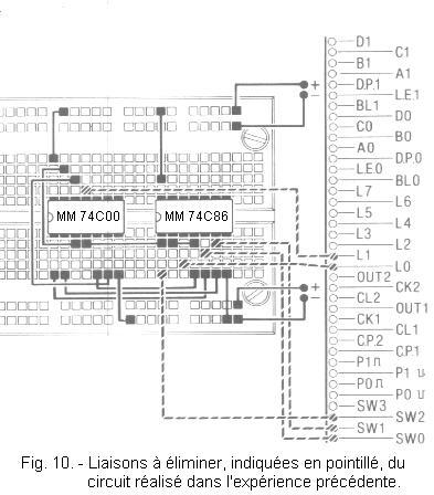
.jpg)
.gif)
.gif)
.gif)
 Click here for the next lesson or in the summary provided for this purpose.
 Top of page
 Next Page