 The limits of use of Digital Integrated Circuits The limits of use of Digital Integrated Circuits |
Offset of the clock
|
The Parasites
|
|
Assembly of Digital Components |
Footer |
The Limits of Use of Digital Integrated Circuits :
2. - NOTIONS ON MICROPROCESSORS
Currently, complex digital systems are made with microprocessors. With the technological progress and the lowering of the cost of integrated circuits, the use of microprocessors has extended to areas where traditional logic circuits used to be used (logic gates, flip-flops, registers, meters, etc.).
The microprocessor is a large scale integrated circuit (L.S.I.) that includes a computing unit processing information provided from outside the system.
These different information processes are determined by a program.
This program consists of a series of operating phases to be executed in a given chronological order.
The working method used is significantly different from that used for the design of traditional electronic circuits.
Indeed, for a traditional assembly, it is simply necessary to determine the logical components (doors, latches, counters, registers ...) necessary to fulfill the desired functions and establish the connections between these different elements.
In a microprocessor-based circuit, it becomes necessary to introduce an additional dimension which is programming, namely that the circuit operates in close relation with the progress of a program.
This type of implementation introduces a new step in the flexibility and in the operating flexibility of digital circuits.
Indeed, just change the program in the memory for the microprocessor system performs new functions.
We can point out the increasing use of microprocessors in today's world (CNC machine tools, IT, telematics, household appliances, road traffic, railways ...).
In addition, the microprocessor has become a standard product since it can fulfill a wide variety of tasks. This has resulted in a considerable reduction in production costs.
In this brief introduction to the microprocessor, we present in Figure 12 the synopsis of a microprocessor encountered in household appliances (washing machines, stoves, etc.).
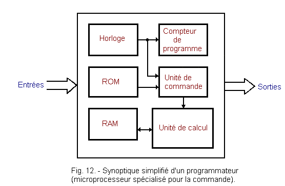
This microprocessor specially designed for controlling simple devices is often called a controller.
The ROM memory has a capacity of one or two kilobytes and contains the work program.
RAM memory has a capacity of a few hundred bits. It is the information relating to the state of the system and the control elements that pass through this memory.
The program is a set of instructions (orders) executable in a given order.
The program counter allows the chronological sequence in the given order of the program.
The computing unit processes the data that reaches it and generates the information needed to complete the program.
The control unit coordinates these different elements.
These programmers can also have other elements (analog-digital converter, real-time clock (timer) ...).
In principle, a microprocessor can process all the functions traditionally performed by a digital circuit. However, the microprocessor system may be too slow to perform certain operations. In this case, it will be necessary to resort to wired circuits (traditional circuits).
In addition, the use of a microprocessor often requires having an associated development system to design the program.
This results in a certain cost of design. This is why in a certain number of cases, it is even more interesting to resort to classic schemes (logic gates, flip-flops, etc.).
![]() 3. - LIMITS OF EMPLOYMENT OF DIGITAL INTEGRATED CIRCUITS
3. - LIMITS OF EMPLOYMENT OF DIGITAL INTEGRATED CIRCUITS
3. 1. - THE MAXIMUM CLOCK FREQUENCY
This is a parameter that must often be considered in the design of digital systems.
When examining the meters, this notion has already been presented. It had become apparent that if certain integrated circuits were made to work at frequencies that were too high, operating randomness or even complete breakdowns occurred in certain cases.
In fact, this notion of limit speed of operation refers to two fundamental data : the propagation time of a signal through a given circuit (logic gates, flip-flops, etc.) and the transition time from a logic state to a logic one complementary logical state (switching or transition time).
It is for these reasons that the manufacturer always specifies the maximum operating speed of an integrated circuit.
This maximum speed (or frequency) is a few MHz for CMOS circuits and a few tens of MHz for TTL circuits.
However, it is good to leave a safe interval and not operate a system (or component) at its maximum allowed frequency. On the other hand, the constructor usually provides two maximum frequency values.
One is the typical value (or average value) which is the maximum frequency at which many of the circuits of the same type can operate. The other is the minimum value : this is the maximum frequency at which we are absolutely sure that all circuits of this type can work. The latter is therefore a little lower than the typical value.
In general, it is necessary to take into account this minimum value and not of the typical value because if one works with this last one, the risk exists that the component can not function correctly.
![]() Consider the following example
:
Consider the following example
:
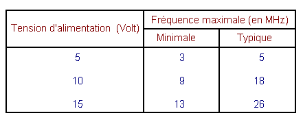
The table below gives the typical maximum and minimum frequencies according to the supply voltage used.
The maximum frequency is related to three factors.
The first, as shown in the table above, is the supply voltage. The maximum frequency increases as the supply voltage increases.
A second factor is the CL charging capability for a MOS output. The maximum frequency also increases when this capacity decreases.
The table in Figure 13 shows the effects of these two factors on the maximum frequency.
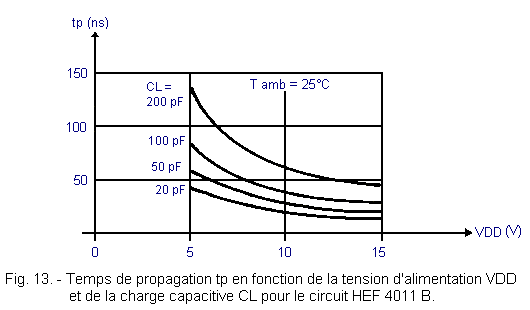
For this, the propagation times tp of the circuit 4011 B were plotted against these two parameters.
The increase in the maximum frequency (equivalent to a decrease in the propagation time) is explained by the decrease in the switching time of the MOS transistors.
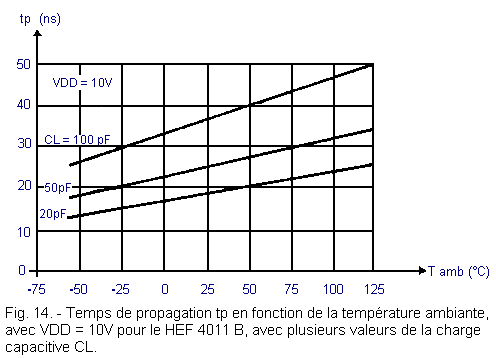
The last factor is the temperature. The maximum frequency increases as the temperature decreases.
The example of Figure 14 is always relative to circuit HEF 4011 B.
Until then, we have considered only one component. Now, in a digital system, there is usually a whole set of connected integrated circuits. Other factors may interfere with the maximum operating speed.
Consider, for example, the circuit of Figure 15 consisting of two synchronous D flip-flops and two NAND gates.
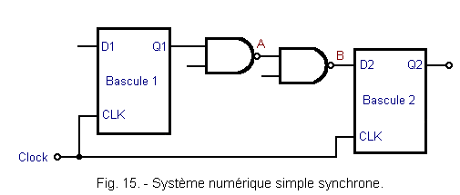
When an active clock edge is present, the two flip-flops switch simultaneously.
The data present on the input D1 is transferred to the output Q1 and the two NAND doors switch one after the other. The data present on the input D2 changes.
Figure 16 shows the various delays that are added, due to the propagation times through the first rocker and the two NAND gates.
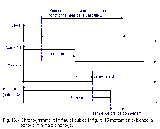
The set up time is the time during which the new data must be present on the input of the flip-flop before the active edge of the clock.
We will calculate the maximum frequency at which this circuit can work.
For this, we calculate the minimum period necessary for its operation.
The D flip-flops are of the 74C74 type, the 74C00 NAND gates and the supply voltage is + 5 volts (when the supply voltage increases, the propagation time decreases).
The first delay (propagation delay) is 300 ns, the second and third delay are 90 ns and the prepositioning time is 100 ns.
The minimum duration of the clock period is therefore equal to the three delay times added to the prepositioning time, that is to say :
300 + 90 + 90 + 100 = 580 ns
The maximum frequency is (1 / 580) x 109 = 1.7 MHz.
This frequency is less than the maximum clock rate relative to the 74C74 flip-flop which is equal to 2 MHz.
If the number of logic gates in series increases, the maximum operating frequency of the circuit decreases.
With 4 NAND doors in series, the period would be worth :
300 + (90 x 4) + 100 = 760 ns
The maximum frequency would be : (1 / 760) x 109 = 1,3 MHz.
It is therefore generally necessary to limit the number of logical gates put in series one after the other.
In cases where this is not possible, additional flip-flops must be inserted as shown in Figure 17.
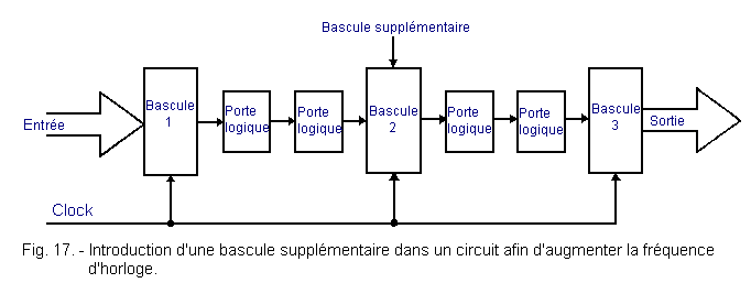
If we maintain the same propagation and prepositioning times as before, we obtain the following results :
In the first case, when the additional flip-flop does not exist :
Minimum clock period = 300 + 90 + 90 + 90 + 90 + 100 = 760 ns.
In the second case, the minimum clock period must be sufficient so that the data present on the input of a flip-flop n can be on the input of the flip-flop n + 1 in the given time.
In the present case, this period is equal to the sum of the propagation times of a latch added to those of the two logic gates, as well as to that of the prepositioning time.
We find :
300 + 90 + 90 + 100 = 580 ns
The additional flip-flop serves as an intermediate storage register for data that travels from the input to the output of the circuit.
This system makes it possible to increase the flow of data through the digital circuit.
![]() 3. 2. - OFFSETTING THE CLOCK
3. 2. - OFFSETTING THE CLOCK
The clock shift (or CLOCK SKEW) is also a problem related to differences in propagation time through logic gates.
The circuit of Figure 18 makes it possible to highlight this problem.
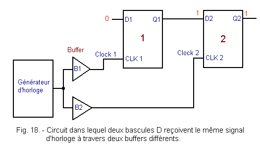
If the propagation times of the two buffers B1 and B2 are very different, there may be a circuit malfunction.
Initially D1 is in state 0 and D2 is in state 1. If the propagation times of the two buffers are identical, the active clock edge is applied simultaneously in CLK 1 and CLK 2, as shown in Figure 19.
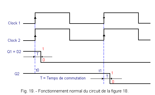
From time t0, Q1 goes to state 0 after a time T which corresponds to the switching time of flip-flop 1. Q2 remains at state 1 since at time t0, D2 is at 1. Q2 only changes state at the next clock edge (time t1).
Suppose now that the buffer B2 has a much longer buffer buffer than B1. There may be a malfunction as shown in Figure 20.
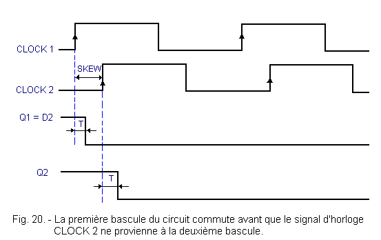
The output Q1 of the first flip-flop is set to 0 before the clock edge reaches the CLK 2 input of the second flip-flop.
The input D2 is therefore in state 0, whereas it should be in state 1 at that moment.
The term «SKEW» represents a «slipping» of the clock signal.
One solution to this problem is to invert the two clock signals as shown in Figure 21.
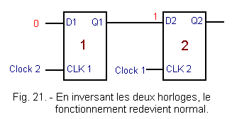
Thus, the second flip-flop will switch a little before the first and we are sure that the initial data present in D2 is transferred to Q2.
![]() 3. 3. - THE PARASITES
3. 3. - THE PARASITES
The parasites are defined as disturbances affecting an electronic signal. The origins of these parasites are innumerable but can be classified in two categories : parasites of natural origin such as those generated by storms for example and parasites of artificial origin such as those produced by an engine.
These parasites can be large enough to disrupt the operation of a logical set. This can be translated concretely by taking into account at a given moment a logic level H instead of a logic level L or vice versa.
In general, efforts will be made to minimize the effects of noise on a logic system.
It should also be noted that a logic unit can work well during the study and test phases performed by the manufacturer and be inoperative once installed at the customer. Indeed, the electronic environment is no longer the same and some physical phenomena that were not taken into account at the time of the design can occur at that time.
These different phenomena can be of electromagnetic nature (radio emission in high frequency, fluorescent tubes ...) or of static nature (electric charges stored in various substrates such as carpets ...).
The technology employed is not without consequence on the effect of these parasites.
The circuits made in MOS technology are much less sensitive to parasites than those made in TTL technology. First, the MOS technology is slower (transition times are longer than for the TTL) and the noise margin is much larger than in TTL. It can reach 45% of the MOS supply voltage, while it is only 0.4 volts in TTL.
For these reasons, in industrial environments with a high risk of parasites, it is preferable to use MOS technology.
There is also a problem related to the adaptation between a transmission line and the load at the end of the line.
The line has a characteristic impedance. This characteristic impedance (Z0) must be substantially equivalent to the impedance of the load if it is desired to limit the signal reflection phenomena.
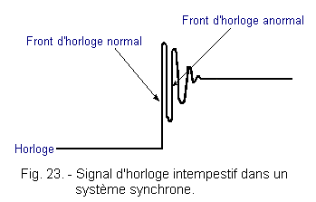
Figure 22 shows an example of reflections on a line that is not suited to the load.
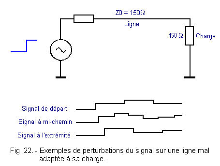
Reflections can create problems for fast circuits (TTL, ECL ...), but also for slow circuits (CMOS).
Bounces may occur in a synchronous system with clock, and they may be considered as a clock signal. This is the case presented in figure 23.
Inductive couplings can also occur between two or more lines.
The transmission lines and the circuit board connections must be as short as possible.
In addition, decoupling capacitors are installed on the power lines near the integrated circuit packages. These capacitors have a value of 0.1 µF at 0.01 µF and absorb the parasites that pass through the supply line (Vcc) and on the ground line.
![]() 3. 4. - THE ASSEMBLY OF DIGITAL
COMPONENTS
3. 4. - THE ASSEMBLY OF DIGITAL
COMPONENTS
You know that digital components belong to different logical families : TTL, CMOS, ECL ..., each having its own characteristics (power supply, propagation time, consumption ...).
Therefore, when it comes to connecting components of different families, their electrical characteristics must be taken into account. In general, it is necessary to insert an interface circuit (= matching circuit) between these components.
An interface circuit is also needed to connect a digital system to the outside world.
Consider first the connections between components of the same family.
In CMOS technology, it is possible to connect a large number of logic gates to the output of another. On the other hand, in TTL, this number is much more limited.
These different notions (entrance and exit) have been seen in the chapters on component technology.
In MOS technology, a logic gate input absorbs or produces (depending on the logic level) a current of 0.005 µA.
An MOS output can provide (or absorb) at least 1.75 mA for a supply voltage of 5 volts (8 mA for 10 volts).
Thus, a MOS logic gate output can theoretically be connected to a number of MOS inputs between 350 000 and 1 600 000.
However, the exit of a MOS gate does not exceed 50 because of the entry capacity of a MOS gate that is 5 pF.
With 50 entries, we get 250 pF.
The propagation time increases significantly with the number of inputs connected to an MOS output.
When going from 50 pF to 100 pF, with 5 Volts of supply voltage, the typical ET gate propagation time goes from 80 ns to 110 ns.
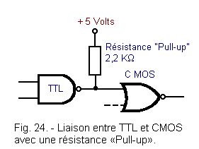
To connect MOS doors to TTL doors, there may be a problem with different supply voltages.
In addition, a TTL output at the H state can be at 2.4 volts, while a MOS input at the H state must be at a potential of 3 to 3.5 volts (for Vcc = 5 volts).
To solve this problem, the TTL output is connected to the power supply through a resistor called «pull-up».
This allows the voltage level to be raised when the output is in state H.
Figure 24 represents two TTL and CMOS gates powered at 5 volts, connected according to this mounting principle.
A MOS output can be connected to a low-power TTL (74 LS) TTL Low Power input (74 L).
In all other cases, MOS circuits having a buffered output and providing a higher current may be used.
If the MOS circuits are powered from a voltage other than 5 volts, it becomes necessary to insert a buffer between the CMOS output and the TTL input, and an open collector buffer between the TTL output and the MOS input (Figure 25).
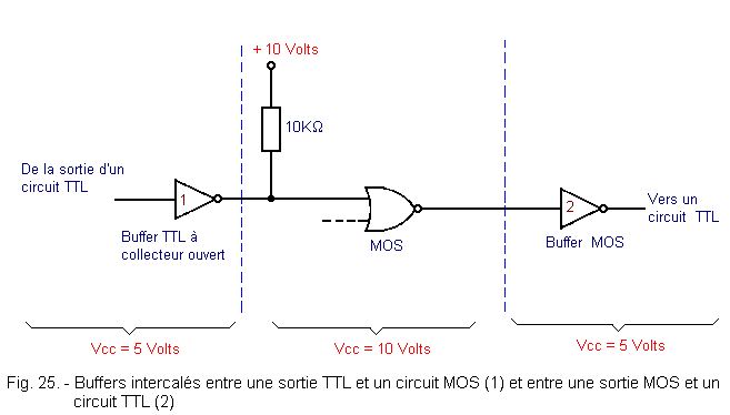
Figure 26 shows the circuit diagram of an open collector TTL buffer.
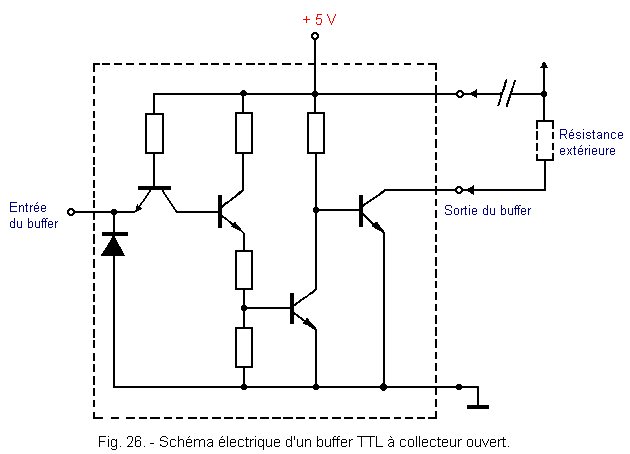
The external resistance is connected to the output of the circuit and the power supply. This supply voltage may be greater than 5 volts.
An open collector gate can also directly control a relay.
Another case to consider is that of Figure 27 where a MOS circuit is supplied between - 5 volts and + 5 volts.
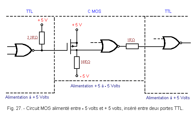
The pin of the MOS circuit, usually wired to ground, is in this case connected to - 5 volts. In such a situation, it is necessary to insert a MOS transistor between the TTL output and the MOS input.
When the TTL output is at the H level, the transistor drives and the input of the MOS circuit is raised to the H level (+ 5 volts). If the TTL output is at the L (0 volt) level, the transistor locks up and the MOS input goes to potential - 5 volts.
Powering the CMOS gate between - 5 volts and + 5 volts provides a higher operating speed than a 5 volts supply.
This theoretical is now over. The next will deal with analog / digital and digital / analog converters.
 Click here for the next lesson or in the summary provided for this purpose. Click here for the next lesson or in the summary provided for this purpose. |
 Top of page Top of page |
|
Previous Page |
 Next Page Next Page |
Nombre de pages vues, à partir de cette date : le 27 Décembre 2019

Envoyez un courrier électronique à Administrateur Web Société pour toute question ou remarque concernant ce site Web.
Version du site : 10. 4. 12 - Site optimisation 1280 x 1024 pixels - Faculté de Nanterre - Dernière modification : 02 Septembre 2016.
Ce site Web a été Créé le, 14 Mars 1999 et ayant Rénové, en Septembre 2016.