We have described it in the previous paragraph. This is a junction. (See semiconductor theory).
It consists of two materials, one of conductivity N, the other of conductivity P.
To these materials are associated two electrodes, ohmic contact (that is to say without creating a parasitic junction).
One connected to the material P, takes the name of anode, the other material N, that of cathode.
Figure 4-a shows the diode as we have schematized so far.
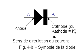
Figure 4-b shows the symbol of this diode as you will see it now in the diagrams of electronics.
What is the purpose of the diode ? We found that, depending on the direction of polarization, she behaved differently. Polarized in reverse, it circulates a tiny current (due to the minority carriers), while, polarized live, a large current (due to the majority carriers) can cross it. In short, it only lets the current flow in one direction.
If we had to make an analogy with fluidics, we would liken it to a non-return valve.
2.1. - CHARACTERISTICS OF THE DIODE
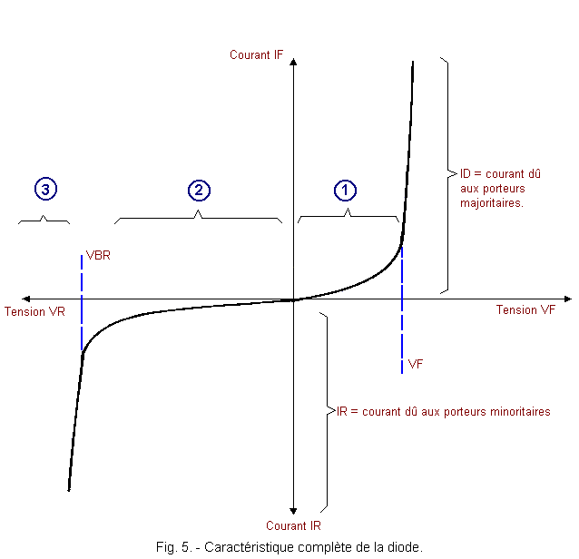
Figure 5 shows on the same graph, the complete characteristic of the diode.
Zone 1 corresponds to the polarization in the forward direction or direct polarization.
The point indicated by VF, corresponds to the predominance of the electric field E, due to the bias voltage, on the electric field e, of the potential barrier and allowing the large free electrons to pass from zone N to zone P.
The current axis represents the direct current ID or current of the majority carriers.
The voltage axis represents the direct voltage applied to the diode.
Zones 2 and 3 correspond to the polarization in the blocked direction, or reverse polarization.
Zone 2 is the inverse characteristic usable for a rectifying diode. In this case, the avalanche voltage VBR must not be reached.
The reverse current is due to minority carriers. In principle in this zone, at fixed temperature, it is theoretically constant, but secondary phenomena tend to slightly increase it.
Zone 3 is marked by the point VBR on the axis of the reverse voltages. It corresponds to an energy transmitted to the minority carrier electrons by the electric field E (generated by the reverse bias voltage), increased by the electric field e (generated by the potential barrier), such that, when arriving in the zone N, tear electrons in the mesh of the network, which in turn, are accelerated by this field and will release other electrons of the mesh before reaching the cathode (electrode of the zone N).
This phenomenon is cumulative, which explains this very significant increase in current, for a negligible increase of the reverse voltage.
In a rectifying diode, not intended to operate in this region, this effect is accompanied by a sharp increase in temperature, which the dimensions of the diode can not evacuate. There is, in this case, destruction of the junction. This is why this point is called the reverse breakdown voltage (VBR = breakdown voltage).
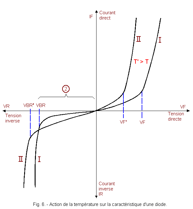
2. 2. - ACTION OF TEMPERATURE
For any increase in temperature, donors in zone N, will lose more easily their excess electron. Therefore, to circulate the free electrons from the N zone to the P zone, the electric field E, generated by the direct bias voltage, may be lower.
The bias voltage will be lower (Figure 6).
The curve I is translated in II where it is noted that VF' < VF for a temperature T' > T.
The rest of the curve hardly changes. As the threshold voltage decreases, it can be interpreted as an improvement of the diode.
In Part 2, the increase in temperature significantly favors the creation of minority carriers, therefore, an increase in the IR current.
This action is more troublesome in this case because it alters the phenomenon of unilateral conduction.
This phenomenon is even more accentuated with germanium, so much so that this defect can be used to detect temperature variations.
The diode we have spoken of so far is called rectifier (for large IF intensities) or signal (when the current IF remains below 100 mA).
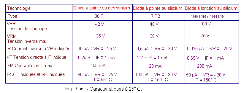
All rectifying diodes are made of silicon and a large part of the signal diodes. However, we still use that are made from germanium, they are called : spikes. The junction is made differently. The table of Figure 6-bis gives the main characteristics of a germanium diode tip, a silicon diode tip and a silicon diode junction.
In this table, for substantially identical reverse voltages, very different reverse currents are observed.
The silicon tip contact diode has a reverse current 60 times lower than in a diode made with germanium. As for the diode junction, silicon, its reverse current is 1200 times lower, but in this case, we must take into account a technological improvement because the latter is of more recent achievement.
It can also be seen that this reverse current is 2 times higher for the diode P1 when the temperature goes from 25° C to 55° C (DT de 30° C).
For diode 17 P2, the reverse current is multiplied by a factor of 200 when the temperature goes from 25° C to 150° C(DT = 125° C). At this temperature of 150° C, this current remains comparable to that observed in a germanium-tipped diode at 55° C. Note that this diode would not withstand a temperature of 150° C.
For the silicon junction diode, there is an increase of this same current by a factor of 2000 for a temperature difference of 125°. This remains lower than the reverse current of the germanium diode at 55° C.
This table does not show the variation of the voltage VF as a function of the temperature, since this kind of diode is used for the signal processing (signal diode). The average operating current being 50 mA, for the diode P1, the voltage VF goes from 0.58 V to 0.55 V.
For diode 1N914B (or 1N4148), the voltage VF goes from 0.9 V to 0.75 V (for IF = 50 mA) when the temperature goes from 25° C to 150° C.
At this current value, we are still far from the maximum value allowed ; this is why in this use, the variation of VF is not of concern.
Finally, note that some diodes support reverse voltages of several thousand volts (VRM = 40 000 V, IF = 3 A, VF = 44 V).
Others are intended for direct currents of several thousand amperes (VRM = 2000 V, IF = 2000 A, VF = 1.35 V, IF for 10 ms = 15 000 A).
2. 3. - DIODES PREPARED FROM REMARKABLE PHENOMENA OF JUNCTION
a) The varicap diode
We know that the potential barrier widens when the junction is reverse biased. This variation is proportional to the applied voltage VR. If we equate this thickness of the barrier with the dielectric of a capacitor, we can say :
- the more the electrodes are separated, the lower the capacitor value (with equal surface and identical material).
In the case of the junction, the more the reverse voltage will increase, the more the potential barrier expands and the more its capacity will decrease.
This corresponds to a VR value of 3 V, for example, at a capacity of the order of 30 pF.
If VR is equal to 3 V, this same capacity takes the value of 30 pF.
This phenomenon is exploited with the varicap diodes (variation of capacity).
In theory, this variation in capacity can range from a few picofarads to a thousand picofarads.
In practice, it is limited from a few picofarads to about fifty picofarads. We can reach a ratio of 6 between the minimum value and the maximum value.
These diodes are used in electronic tuning systems (PLL circuits with voltage controlled oscillator) or frequency multiplying systems.
b) The zener diode
The avalanche voltage, which we know now, is used in some diodes to serve as a reference voltage.
This phenomenon is reversible, provided that the cumulative effect does not lead to the destruction of the junction by heating.
The physicists knew how to limit this heating by a proper doping and a particular geometry of the junctions.
It should be noted that for these diodes, two effects are used :
the zener effect for very low voltages (less than 6 V)
the avalanche effect beyond 6 V.
If a reverse current corresponding to the crossing of the avalanche threshold is injected into such a diode, significant variations in this current will result in a substantially constant voltage across the diode as long as the voltage remains above the voltage avalanche.
These diodes will therefore be used as reference elements in regulated DC voltage supplies.
They will be used in clipping systems. The signal applied to these diodes is not affected until it reaches the zen threshold or elbow. Beyond, the impedance of the diodes becoming very weak, the signal is clipped.
The zener voltage of some of these diodes can reach several hundred volts. Others are made for reverse currents of several amperes.
c) Photodiodes - photocells
In semiconductors, thermal agitation is a creative source of electron / hole pairs. Another energy can lead to the same result : light.
A diode, polarized in reverse, is the seat of a very weak current due to the minority carriers. If, in the housing of this diode, a window is practiced, the light that reaches the junction increases the number of minority carriers. This increase results in a rise in the reverse current.
We are in the presence of a light radiation detector. It's the photodiode.
The reverse current and the conduction current due to the electric field e
generated by the displacement of the majority carriers.
In a junction, the distribution of ionized atoms creates an electric field e.
They act like the voltage of a battery. If a voltmeter whose impedance is high enough is placed at the terminals of the junction, this voltage can be appreciated.
When a luminous radiation strikes the junction, if the reverse current tends to increase, everything happens as if the creative tension of the field e becomes greater. This increase is highlighted by the voltmeter. If the circuit outside the junction has a sufficiently large impedance, we can see the effect of solar cell.
d) LED diode
Polarization in the forward direction is accompanied by light emission.
The diffusion current of the majority carriers, results in the displacement of free electrons of the zone N towards the zone P where they recombine with the holes of this zone, while entering the mesh.
According to the materials, these recombinations are accompanied by a proton emission, whose vibration frequency, specific to the material, leads to light emissions of different colors. This is the principle of the LED (Light Emitting Diode which means light emitting diode).
e) The tunnel diode
It is a highly doped semiconductor and has a very thin junction.
They drive in reverse and live up to a certain IF value. Then when VF continues to increase, IF decreases. It is this negative resistance range that is used, among others, in UHF amplifiers or in very fast switching.
f) The Schottky diode
It consists of a semiconductor and a metal. It has a very low junction capacity, it finds its use in very high frequency circuits.
g) P.I.N. diode
It is characterized by a high avalanche voltage VBR. The capacity of the junction remains very low and the parasitic series resistance is a function of the period of the signal applied. It is used for this phenomenon in high frequency modulation circuits.
All these components are practically used in digital electronics, they were even at the origin of some complete logic systems (logic diodes).
Photodiodes associated with LEDs are widely used in so-called opto-coupler systems.
These make it possible to galvanically isolate circuits whose potentials are very different.
The optical fiber associated with these two elements makes it possible to carry digital information in very disturbed or high-risk environments (dust, coal, etc.).


 Footer
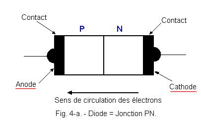
 Click here for the next lesson or in the summary provided for this purpose.
 Top of page
 Next Page