8. - FOURTH EXPERIMENT : OPERATING TEST FOR SYNCHRONOUS SERIAL DATA TRANSMISSION
In the previous experiment, you saw how it is possible to load a register and shift its contents to a single output.
In this manipulation, you will load information on the state of eight inputs in a shift circuit, transmit them on a single wire and find them all eight in parallel on another register placed at the end of the line transmission.
8. 1. - REALIZATION OF THE CIRCUIT
a) Remove from the matrix the integrated circuit MM 74C165 and all the connections relating to the previous experiment.
b) Insert on the matrix the integrated circuits MM 74C164 and MM 74C165 in the position indicated in Figure 36-a and make the connections illustrated by this same figure.
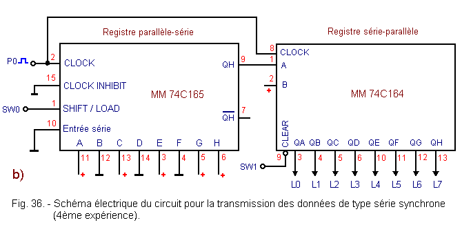
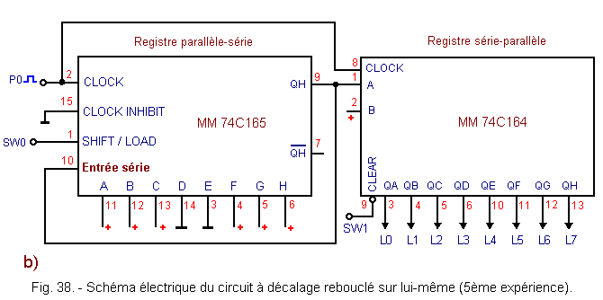
Figure 36-b shows the wiring diagram of the circuit you made.
As you can see, the parallel inputs of the MM 74C165 register are positioned at specific logical levels.
The two registers are placed next to each other for reasons of space and convenience. In reality, however, they are often far from each other for the remote transmission of information. So you have to imagine a rather long link that goes from the QH output of the first register to the input A of the second one.
Since the two registers are controlled by the same clock signal, it is necessary to have a second connecting wire which combines the two CLOCK inputs : for this reason, the transmission is said to be synchronous.
Often, two different clocks are used, one for transmission and another for reception. In this case, it is the transmitted signal, itself, that synchronizes the reception. This type of transmission is said to be asynchronous.
c) Insert the plug into the mains socket and turn on the digilab.
d) Set SW0 to the 0 position. The parallel-serial register then operates in LOAD mode and the levels present on the parallel inputs are loaded on the outputs of the different flip-flops.
e) Set SW1 momentarily to position 0, then return it to position 1 : all eight LEDs are off.
Indeed, as you can see in the diagram of the circuit, you apply in this way a level L on the entry CLEAR of the serial-parallel register. All exits therefore go to level L ; the register is initialized or reset.
f) Switch SW0 to position 1 : the parallel-serial register is ready to operate thus in SHIFT mode.
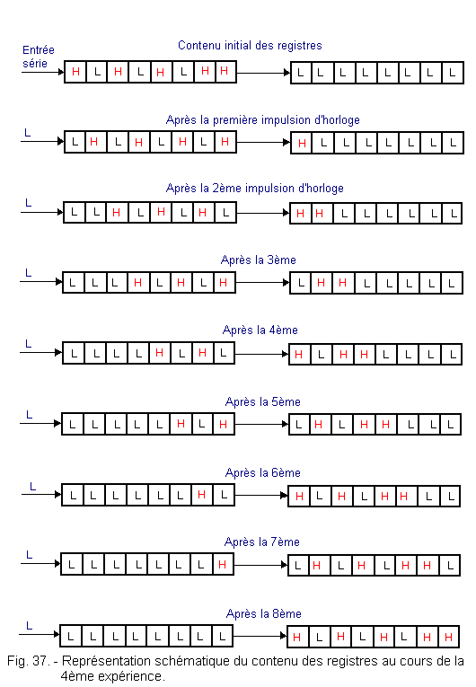
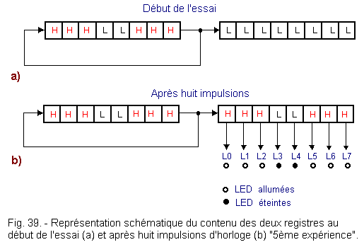
The current contents of the two registers are shown schematically in Figure 37 (first line).
g) Press P0 : L0 lights up. Indeed, the contents of the eighth flip-flop of the first register has been transferred to the first flip-flop of the second register. All other information has also shifted one floor.
The first stage of the parallel-series register is loaded by a level L since the serial input is connected to ground (Figure 37 - 2nd line).
h) Apply another seven clock pulses using the P0 button : at each clock pulse, you notice a shift of one row to the right of the information, as shown in Figure 37.
At this moment, all the content of the first register has moved into the second one, which you notice by observing the LEDs that are in the following situation :
L0 lit
L4 lit.
L1 extinguished
L5 extinguished
L2 lit
L6 lit
L3 extinguished
L7 lit
i) Continue to operate P0 ; after eight clock pulses, all the LEDs are off.
The second register has in fact loaded all the levels L which come from the serial input of the first register.
j) Turn "OFF" the power switch and remove the plug from the power outlet.
With this experiment, you have verified the principle on which the transmission of synchronous serial type information is based.
The logic information is transmitted by a "transmitter" circuit on a single wire through a parallel-serial register. They are received by a "receiver" circuit which is a series-parallel register.
The first register takes the information in parallel and transmits them one after the other in series, the second receives them one after the other and then presents them simultaneously in parallel.
Naturally, it is necessary to know the exact moment when the information must be recorded on the outputs of the "receiver" register. In our case, we counted the number of clock pulses applied to the circuit ; at the eighth pulse, you observed the outputs of the second circuit and made sure that they matched the inputs of the first circuit.
In reality, this counting is done automatically by appropriate circuits which signal that all the information has arrived, thus available for reading.
9. - FIFTH EXPERIENCE : STUDY OF THE FUNCTIONING OF A REGISTER WITH SHIFTING REACHED ON HIMSELF
With this manipulation, you will check how it is possible to keep the information contained in a shift register.
In the previous experiment, you saw that the contents of the parallel-serial register MM 74C165 were transferred to the serial-parallel register MM 74C164 and that after this operation, the parallel-serial register had lost its contents.
During this experiment, you will see how you can keep the information on the place of transmission as on the place of reception by looping back on itself the first register so that the information circulates permanently.
9. 1. - REALIZATION OF THE CIRCUIT
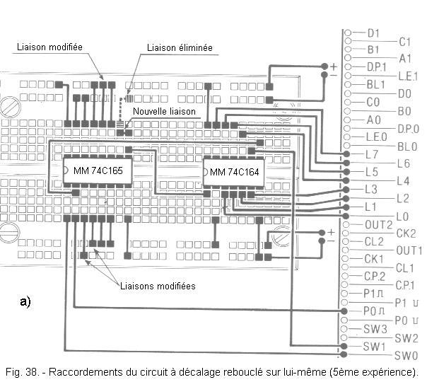
Modify the circuit connections related to the previous experiment, as shown in Figure 38-a and specified below :
Disconnect from the ground the inputs B and F (pins 12 and 4) of the integrated circuit MM 74C165 and connect them to the "+".
Disconnect the "+"
input E (pin 3) from the MM 74C165 and connect it to the ground.
Unplug the serial input (pin 10) from the MM 74C165 and connect it to the QH output (pin 9).
With these new links, you simply changed the logical levels applied to the parallel inputs of the parallel-serial register. In addition, you have connected its output to its serial input as you can see in the wiring diagram in Figure 38-b.
9. 2. - OPERATING TEST
a) Place SW1 on the 0 position, insert the plug into the socket and turn on the digilab : all the LEDs are off as the CLEAR input is activated.
b) Put SW0 first on position 0, then on position 1 : you have thus loaded the parallel-serial register. The contents of both registers are shown in Figure 39-a.
c) Put SW1 on position 1 and press P0 : LED L0 lights up.
d) Press seven more times on P0 : you notice that the second register has received all the contents of the first, which is indicated to you by the state of the eight LEDs.
Until then, everything went as in the previous experience. The current contents of the registers are shown in Figure 39-b.
e) Operate P0 several times : you notice that the LEDs do not go out as in the fourth experiment, but continue to turn on and off as the information is shifted.
Indeed, the first register retains its contents, because its output is looped back on its entry.
Now, instead of shifting the information by means of P0, it will be shifted automatically by the clock signal provided by the digilab oscillator.
f) Turn off the power by putting the switch in the "OFF" position.
g) Set SW0 and SW1 to the 0 position.
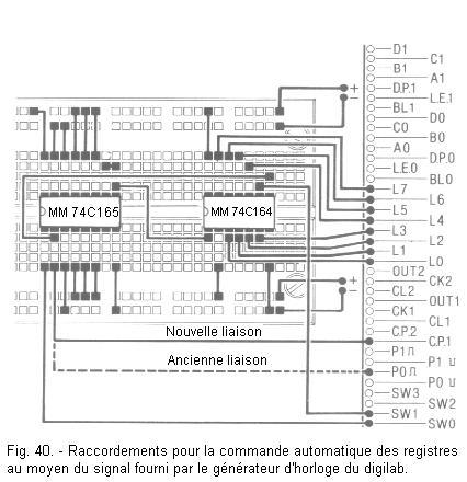
h) Modify the connection between pin 2 (CLOCK) of the integrated circuit MM 74C165 and contact P0
by moving it on the contact CP1 as shown in Figure 40, where the previous link is shown in dashed line.
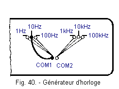
i) Connect the COM1 contact of the first digilab clock generator with the contact indicated by the 10 Hz marking. (See Figure 40).
Thus wired, the generator provides a rectangular signal with a frequency of 10 Hz. This same rectangular signal, through the contact CP1, is applied to the CLOCK inputs of the two registers ; in this way, the progress of the information in the registers will no longer be controlled manually via the button P0, but automatically by the pulses of the clock generator.
j) Feed the digilab and put SW0 on position 1 : the first register is loaded and the LEDs are off since SW1 is on position 0.
k) Now put SW1 on position 1 : the outputs of the serial-parallel register are no longer forced to state 0. This register starts to load and at each clock pulse, you see the information shift as shown by the switching on and off of the LEDs.
With the procedure described above, you can shift any combination of LEDs on or off. To do this, simply change the levels applied to the parallel inputs and then load them into the parallel-serial register.
In conclusion, this experiment shows you how to keep the information inside a register by simply connecting the output to the input.
Everybody knows the luminous inscriptions which parade by repeating themselves periodically: the operation of the circuits with which these plays of light are realized is based on the same principle as the shift registers looped on themselves.
In addition to those experienced in this practice, there are other types of registers, described in a later theory, such as dynamic registers.
In the next practice, you will examine the counters and frequency dividers.


 Study of the operation of an Offset Register Rejoined on itself
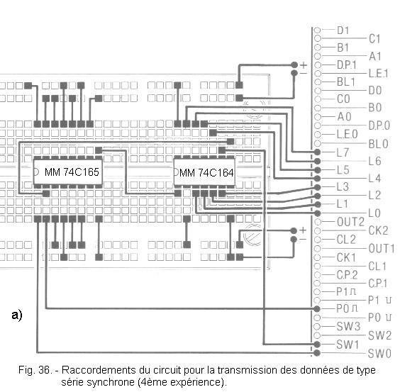
 Click here for the next lesson or in the summary provided for this purpose.
 Top of page
 Next Page