Mounting the Pushbuttons and Testing the R-S Rocker :
3. - ASSEMBLY OF THE GROUP BUTTONS - PUSH
First, remove all links made in the first experiment. Then replace the integrated circuit MM 74C00 in the graphitized foam.
Now take the work on the digilab, proceeding to the assembly of the group pushbuttons.
a) Place one of the pushbuttons on the printed circuit board above the P0 symbol (Figure 4-a). The flat part of the cylindrical upper part is opposed to the inscription P0. The indications NC, NO, C, marked on the base of the push-button must correspond to those printed on the printed circuit board (Figure 4-b).
b) Make sure that the push button is pushed all the way onto the plate and weld the seven terminals.
c) In the same way, solder the second push-button at P1 (Figure 4-a).
d) Check the ohmmeter resistance R26, R27, R28 and R29 (4.7 kΩ, 1 / 4 W, 5%), "yellow, purple, red, gold" and weld these four resistors to the locations indicated on the epoxy wafer (Figure 4-a). Follow the advice given previously for mounting the resistors.
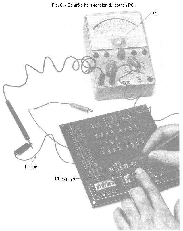
3. 1. - OFF-VOLTAGE CONTROL
Use the controller on the Ω X 1 000 gauge and refer to the indications in the table in Figure 5.
NOTE : The ground corresponds to the black power cord clamp.
Fig. 5. - Off-line control of the pushbutton group.
N°
Connection points of the ohmmeter
Position of the push buttons
Values obtained
1
Between R26 side P0 and mass
P0 supported
P0 released
0 W
6,3 at 7,7 kW
2
Between R27 side P0 and mass
P0 supported
P0 released
6,3 at 7,7 kW
0 W
3
Between R28 side P0 and mass
P1 supported
P1 released
6,3 at 7,7 kW
0 W
4
Between R29 side P0 and mass
P1 supported
P1 released
0 W
6,3 at 7,7 kW
Perform the first check by connecting the black tip to the crocodile clip on the black power cord and touch the other terminal to the pushbutton group of R26 (Figure 6).
By pressing the P0 button, you must find a zero resistance value, while releasing this pushbutton you must find a resistance value between 6.3 and 7.7 kΩ.
Then carry out the following checks, touching the points indicated in the table Figure 5 one after the other. If you do not obtain the expected results, check the welds made, make sure there are no short circuits between neighboring copper tracks and that the pushbuttons were mounted correctly.
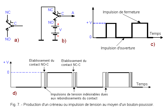
The pushbuttons you have mounted work as inverters, each with three terminals. The central terminal marked by C is the common terminal, in contact with the NC terminal when the button is at rest (button released). By pressing the button, terminal C contacts the NO terminal (Figure 7-a). This type of button is particularly suitable for generating control pulses of longer or shorter duration.
For this, it would be sufficient, at first sight, to realize the simple circuit shown in Figure 7-b. At rest, terminal A is at potential 0 volt. By pressing the button, terminal A is at potential + V.
The voltage on terminal A with respect to the ground is represented theoretically in Figure 7-c under both conditions, button at rest and button depressed.
In practice, things are different. The push button is not a perfect mechanical device and the metal contacts bounce back and forth several times at closing. In practice, the voltage on terminal A varies as shown in Figure 7-d. The amplitude, duration and number of rebounds generated depend on the characteristics of the push buttons and the circuit to which they are attached.
These voltage pulses created at the closing of the C-NO and C-NC contacts are very generally undesirable for the electronic circuits. To avoid this disadvantage, use the flip-flop circuit previously examined. To test this use, do the following :
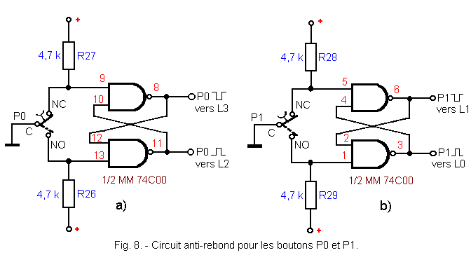
a) Insert the integrated circuit MM 74C00 in the support IC1. With the hard-wired resistors R26, R27, R28 and R29, you get the two identical anti-bounce circuits shown in Figure 8.
The two outputs of the debouncing circuit (Figure 8-a) are in contact with the contacts of the group of connectors designated by the inscription P0
and P0.
Those of the circuit (Figure 8-b) are connected to the connectors designated P1
and P1. For each push button, the NC and NO marks indicate the contacts in connection with the common terminal C in both positions, button released, button pressed.
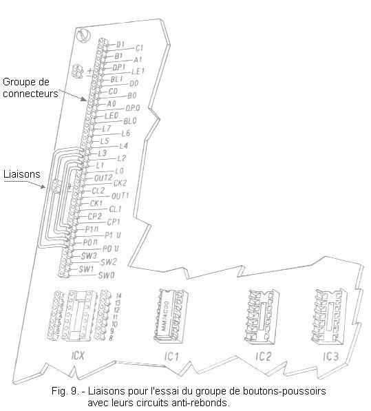
b) Now perform the connections shown in Figure 9. You connect the four outputs P0,
P0,
P1,
P1
respectively to the four LEDs L3, L2, L1, L0. Connect the power supply (battery). You observe that the L0 and L2 LEDs are off while the L1 and L3 LEDs are lit.
Indeed, you find one of the cases seen inFigure 3. The input 9 of the circuit MM 74C00 is in the state L (rest position of the button P0) and the input 13 is in the state H thanks to the resistance R26 connected to the positive voltage (Figure 8-a). So the output P0is in state H and L3 on ; the output P0
is in state L and L2 extinguished.
Now perform the following test with P0.
c) Press the P0 : L2 lights up
and
L3 goes out. The P0 button is in the position shown in dotted lines in Figure 8-a.
The input 9 of the flip-flop is thus carried across the resistor R27 at the level H, while the input 13 is brought to a level L thanks to the pusher P0.
There is thus switching of the exits, P0
passes to the state H and P0
to the state L.
d) Release P0, you find the previous situation, that is to say L3 on and L2 off. In this way, a pulse is produced on the output P0
and its duration is equal to the time during which the button P0 remains depressed. This pulse is negative because the output in state H goes to level L then returns to state H. It is designated by the symbol .
Simultaneously, a positive pulse occurred on the output P0; this L level output went to H level and then returned to L level after a while. This positive impulse is indicated by the symbol .
The Figure 7-c shows these two pulses as you could see them by means of an oscilloscope. There is no rebound phenomenon due to mechanical contact.
Indeed, when you pressed the P0 button, as soon as the contact was established for the first time between C and NO, the flip-flop changed state. The contact broke several times before being definitive, however these successive rebounds of the contact C-NO did not cause a change of state of the latch which memorized the first passage in the state L of its entry 13.
The process is the same when you release P0 and the contact between NC and C is established.
You thus obtain voltage pulses on the outputs very close to the ideal pulses shown in Figure 7-c, furthermore the transition from a logic level to the complementary level is very fast because linked only to the very short switching or transition speed of the rocker.
e) You can perform the same tests with the second scale shown in Figure 8-b.
If the circuit does not work as expected, check the connections made and the continuity of the copper tracks of the printed circuit.
If necessary, you can finally replace the integrated circuit MM 74C00 with the other identical circuit in your possession.
Now leave the MM 74C00 permanently inserted in the IC1 socket to use the two debounce circuits.
You will have on the digilab two pulse generators which will be used to control the logic circuits that you will realize thereafter. This will allow you to have pest free pulses.


 An Application of the RS Flip-Flop
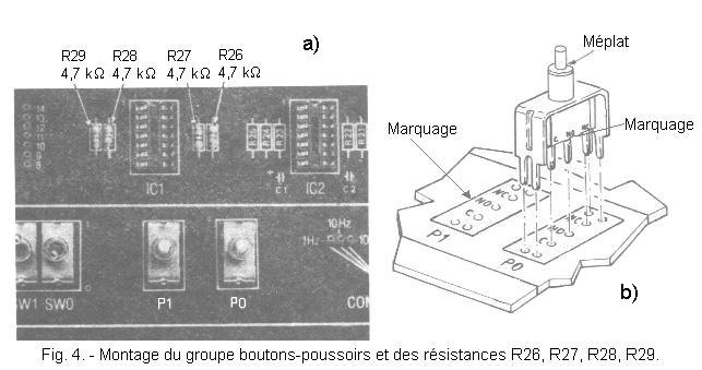
 Click here for the next lesson or in the summary provided for this purpose.
 Top of page
 Next Page