8. - SIXTH EXPERIENCE : EMPLOYING MEMORY TO GENERATE SEQUENCES
We often see luminous signs on which the inscriptions move, turn on and off according to a programmed sequence. The circuits to achieve this are numerous and you have already seen one in the theory devoted to shift registers. In this experiment, you will use memory to accomplish the same job in a more flexible way as it is easily programmable.
8. 1. - REALIZATION OF THE ASSEMBLY
a) Remove the connections between the inputs of the buffer 74LS245 (pins 2, 3, 4, 5, 6, 7, 8, 9) and the ground as well as the dotted line shown in Figure 41, without however changing the other connections. Make sure pin 21 of memory HM6116P-4 is connected to SW0 and not to pin 10 of the CD4040 meter.
b) Insert the integrated circuits MM74C163 (synchronous bit counter of module 16) and MM74C193 (synchronous decimal counter) into the positions indicated in Figure 41.
Then perform the bindings.
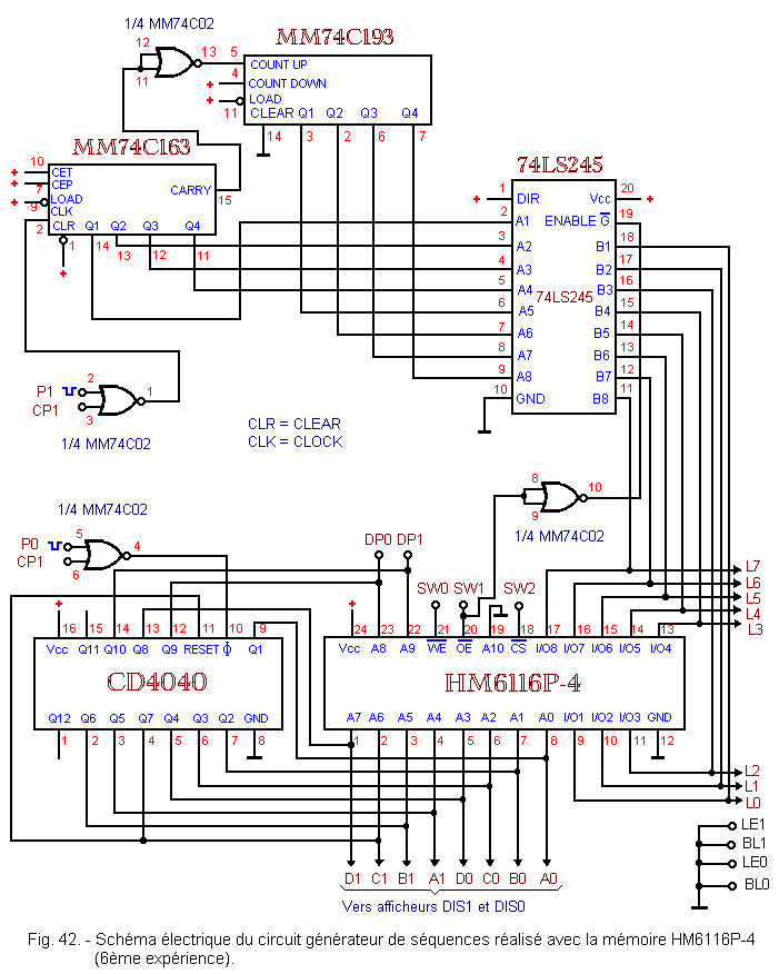
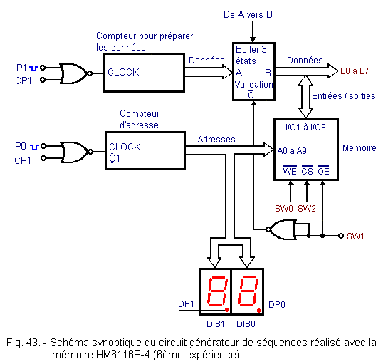
The Figures 42 and 43 respectively show the electrical diagram and block diagram of the circuit that you have just realized.
As you can see, two counters have been added ; they are cascaded and form an 8 bits counter. The clock signal that controls this counter comes from the contact CP1. The P1 button validates when the CP1 switch is pushed through a NOR gate.
The two counters are used to compose the data to be written in a more convenient way than with the system used previously.
It suffices to press P1 so that the counters increment more or less rapidly, according to the frequency of the clock signal, until the outputs of these give the desired value, which is then written in memory by the usual procedure.
In addition, the address counter has been modified to count in module 64. This is obtained by connecting the output Q7 with the RESET so that when the number 64 (1 000 000 in binary code) is reached, the counter returns to 0.
The accessible memory positions in which 8 bits data can be read and written are therefore 64 in number.
8. 2. - OPERATING TEST
It is to write in memory data such as, read after, they allow to turn on the LEDs according to a pre-established program. To do this, simply proceed in the following order :
Preposition the memory.
Prepare the data.
Write the data to the prepared address.
Increment the address of a step.
Prepare the new data.
Write the new data.
Proceed in the same way to the last available address, that is to say 64 since at the next clock stroke, the address counter returns to zero.
To write the data into memory, it is necessary to perform the operations listed below :
The address is formed by pressing P0 to the value of the desired address. This is read on DIS0 and DIS1 displays.
The data is prepared by pressing P1 until the LEDs display the desired value of the data.
The data is written by switching SW0 from position 1 to position 0 and then returning it to 1 again.
Proceed as follows :
a) Put SW0 on position 1.
b) Set SW1 to position 1 (you inhibit the memory output).
c) Set SW2 to position 0 (you enable the memory).
d) Turn on the Digilab.
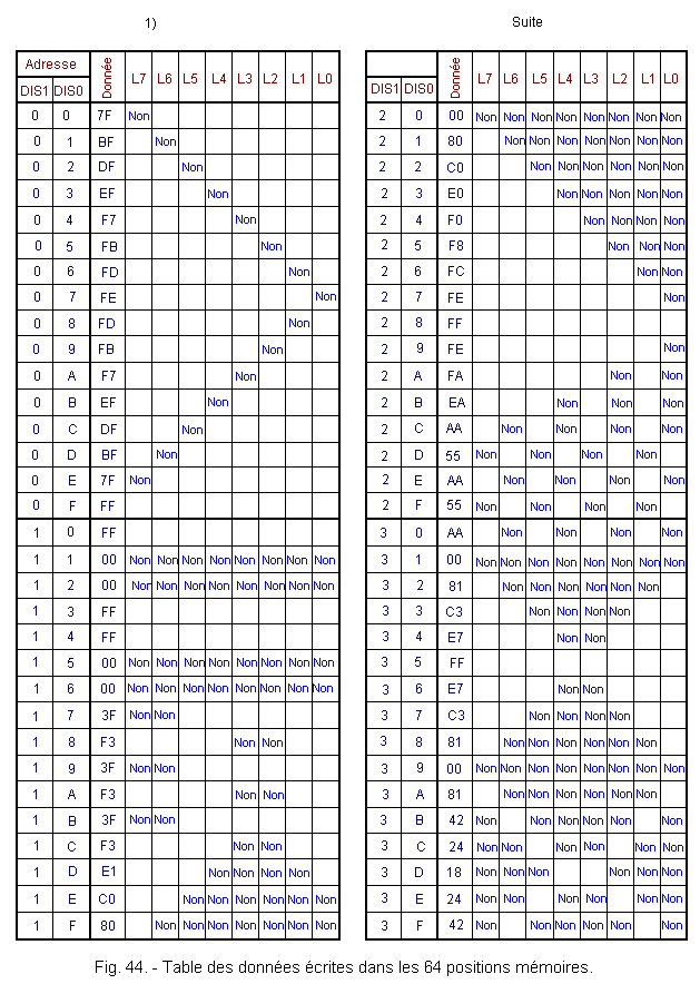
e) Write in memory the data shown in the table of Figure 44.
In the first two columns of this table is reported the address as it appears on DIS0 and DIS1 ; in the third column is indicated the hexadecimal value of the data and in the other eight columns, the value of the data as read on the LEDs ("NO" indicates that the corresponding LEDs are off, while the empty boxes mean that the corresponding LEDs are lit).
Now check if the data is written in memory.
f) Set SW0 to position 1, so you allow playback.
g) Put SW1 on position 0 : the output of the data is validated. Leave SW2 on the position 0.
h) Set the address counter to address 00.
i) Examine the LEDs : they should all be lit, except for L7, as shown in the first line of the table in Figure 44.
j) Continue reading the data, the address is incremented step by step.
k) Check the accuracy of the data by holding P0 down :the LEDs flash in the programmed sequence. This sequence continues until you release the button.
If you want to increase the speed, simply change the frequency of the clock signal from 1 Hz to 10 Hz.
l) At the end of the experiment, switch off the Digilab.
Remember that by unplugging the power, all data written to memory is lost.
In this manipulation, you have realized a sequential system with programmed logic stored in a memory.
This type of application is particularly important because the LEDs can be replaced by various control circuits such as relays operating machine tools, or to achieve any system whose operation must be controlled sequentially.
Currently, microprocessors are widely used for these commands, but it is not always worth investing money and wasting time for the development of a microprocessor project. In such cases, a stored-sequence control circuit is the most advantageous solution.
Volatile memories, of the type that you used in the experiments of this practice 12, are used only when it is necessary to change sequences almost continuously. If on the other hand, the sequence is always the same or is very rarely changed, it is appropriate to use non volatile memories called ROM such as ROM or EPROM.


 Footer
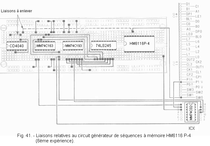
 Click here for the next lesson or in the summary provided for this purpose.
 Top of page
 Next Page