Examining the Operation of a Memory Reading / Writing of Static Type :
5. - THIRD EXPERIENCE : EXAMINING THE OPERATION OF A STATIC-TYPE READ / WRITE MEMORY.
In this manipulation, you will use the integrated circuit HM6116P-4 which is a read / write memory type RAM, that is to say random access ; which means that access to each memory cell is possible directly without any pre-established order. The time required to read or write data in a cell (or access time) is therefore independent of the address thereof, which is not true for a serial access memory.
The typical access time is 200 ns.
The memory capacity is 2K x 8, so it contains 2048 x 8 = 16 384 memory cells.
These are arranged in groups of eight ; that is, 8 bits are written or read simultaneously. They constitute an 8 bits memory word generally called Byte. It is commonly said that such memory is a memory of 2 K Byte (pronounced Kilobait).
The integrated circuit considered is made in CMOS technology and requires a power supply of 4.5 V to 5.5 V.
Supply voltages greater than + 5.5 V may irreparably damage the integrated circuit, while with voltages below + 4.5 V, normal operation is not guaranteed.
The component in question is relatively complicated to use, even if its principle operation is simple. As a result, the experiments that follow will provide editing of a certain complexity.
However, if you scrupulously follow the instructions provided, you will have no problem.
Let's first see what are the characteristics of the memory you will use.
5. 1. - MEMORY DESCRIPTION RAM HM6116P-4
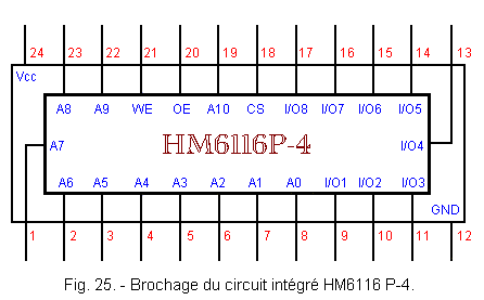
The simplified block diagram of the memory in question is shown in Figure 24. Its pinout scheme is shown in Figure 25.
Examining the block diagram, we first notice eleven address entries, marked by the letters A0 to A10.
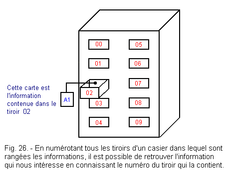
In the theory 12, digital electronics, you have seen that to be able to write or read data in a memory, it is necessary to address it, that is to indicate in which cell or group of cells the data must be read or written.
Indeed, a memory is formed of very many cells arranged in rows and columns similarly to the drawers of a storage unit such as that shown in Figure 26. The furniture shown in this figure is very small and has only ten drawers ; each drawer is marked with a number and contains information.
The information can be written on cards stored in the different drawers ; when it is necessary to recover one of the information, it is necessary for the one who must take it, to know the number of the drawer which contains it.
In the same way, to read or write in memory one of the 2048 words of 8 bits that it can contain, it is necessary to indicate the address. For this purpose, we use the address entries which are eleven in number, since with 11 bits, we can obtain 2048 different combinations : 211 = 2048.
Let us continue the examination of the diagram of Figure 24. We can see the memory proper and its stages of entry and exit. It can be seen that, depending on the function to be performed, the same terminals serve as input and output. the input / output terminals are marked with I / O1 to I / O8 (I / O for Input / Output).
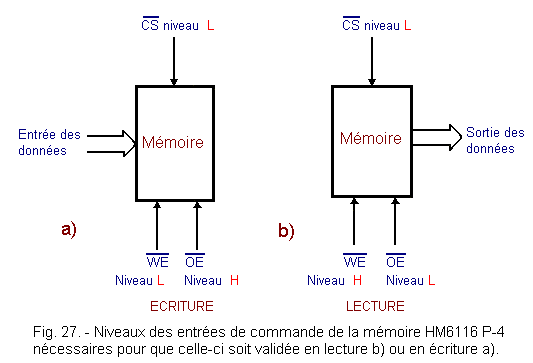
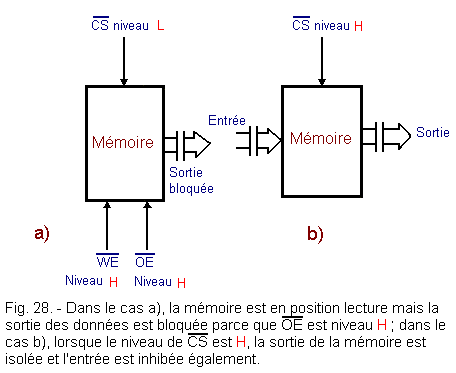
The order of writing or reading is given by means of the command signal; when this input is at the L level, the memory is prepositioned for writing ; the I / O terminals are therefore input terminals ; if against
is at level H, the memory is prepositioned for the reading and the I / O terminals are output terminals.
Two other command entries are also planned
and .
The first validates or prohibits the exit; indeed,
stands for Output Enable. When it is at the L level, it is possible to read the data in the memory.
When it is at level H, the output is forbidden and isolated ("high impedance").
Indeed, this integrated circuit as the bidirectional buffer of the first experiment is of the TRI-STATE type. Thus, one can connect several memories on a single bus.
The other command entry allows or inhibits access to the box ;
means Chip Select, that is to say box selection.
When
is low, the memory is selected and you can read and write as needed ; when this entry is at the high level, you can not read or write to the memory.
Figure 27 shows the two cases : read and write.
In Figure 28, on the other hand, one can see the case where the state of the entries of validation does not allow reading or writing.
5. 2. - REALIZATION OF THE ASSEMBLY
a) Remove all links for the previous experiment and remove the IC from the contact matrix.
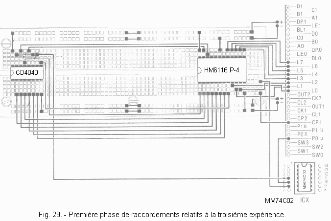
b) Insert on the matrix the integrated circuits HM6116P-4 (RAM 2 K x 8) and CD 4040 (12 bits counter) in the positions shown in Figure 29.
c) Insert the integrated circuit MM 74C02 (4 NOR gates) on the ICX bracket.
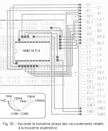
d) Complete the assembly by making the connections indicated Figure 29 and Figure 30.
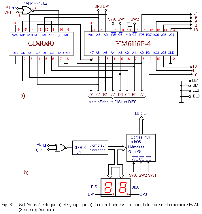
The electrical diagram of the assembly carried out and the corresponding block diagram are indicated in Figure 31.
The editing you have done includes the previously experimented 12 bits counter, modified so that it only has 10 bits left. What we do, connecting the Q11 output to the RESET input.
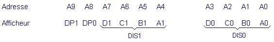
The counter outputs are connected to the "address inputs" of the memory. In this way, the counter selects the memory box that must be read or written. Its address can be read on the two displays DIS0 and DIS1 by respecting the following correspondence :
The bit of the address A9 is represented by the decimal point DP1 of the display DIS1 ; the bit A8 is represented by the decimal point DP0 of the DIS0 display.
These two points are two LED indicators that light up when the bit is 1 and go off when it is 0.
The bits A7 to A4 are displayed in hexadecimal form on DIS1, those of A3 to A0 are given by DIS0.
Note that only ten of the eleven memory addressing entries are used here ; indeed, the pin 19 corresponding to the input A10 is connected to the ground and is permanently at the level L.
Thus, the capacity of the memory is only half exploited which brings it back to 1 K x 8 bits, see 1024 x 8 = 8 192 bits.
This limitation of use, imposed by the number of indicator lights available on the Digilab, is advantageous in practice, because it makes it simpler and faster operation of addressing the memory.
One may wonder why a counter is used to address the memory. The reason is simple : the Digilab does not have enough switches for this, it would take ten, as many as there are address bits.
In this case, the use of a counter is very convenient because one can scroll automatically the addresses of the memory one after the other.
The NOR gate, located at the entrance to the meter, serves this purpose. According to the level P0,
it lets pass or blocks the rectangular signal delivered by the clock and available in CP1.
The data entering or leaving the memory are displayed by the eight LEDs L0 to L7, according to the usual convention : the 1 is indicated by a lit LED and the 0 by an LED off.
This first attempt of the memory concerns the reading of its contents.
a) Turn on the Digilab and observe the displays : they indicate any number that depends on the state (random) to which the counter passes at the moment of power-up. This number indicates the memory address that is being examined.
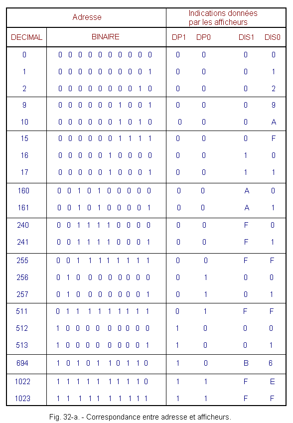
In the table of Figure 32-a are shown some examples of the correspondence between the address and the numbers read on the displays. A 1 in the columns of DP1 and DP0 indicates that they are lit, a 0 indicates that they are off.
The decimal translation of the address from the hexadecimal value given by the displays is not difficult ; just translate the hexadecimal number into a binary number and then convert to decimal.
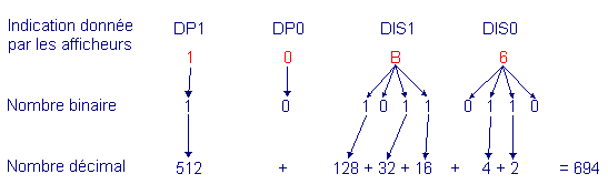
For example, the address 10B6 corresponds to :
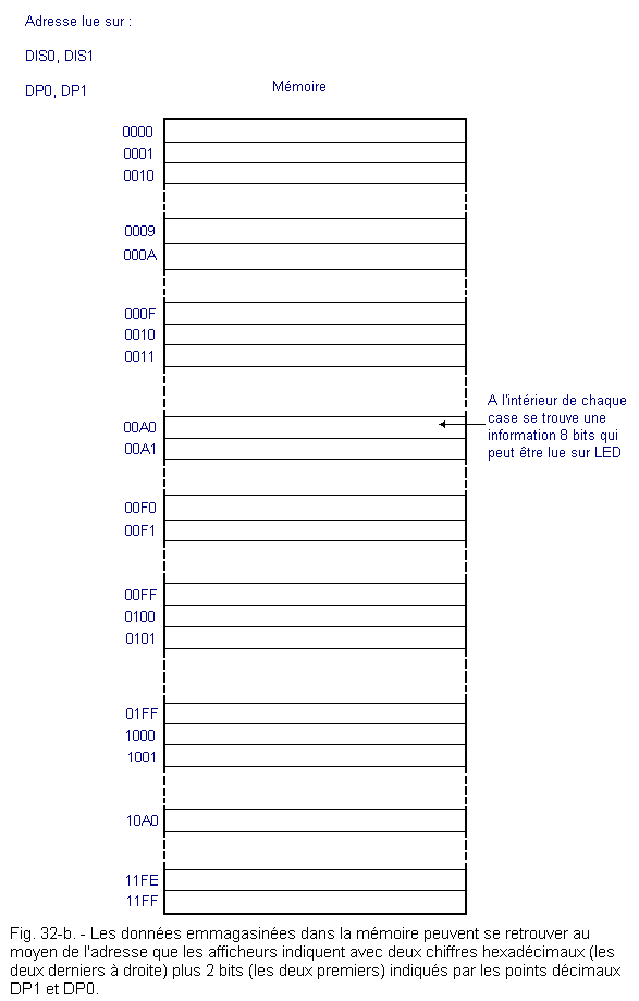
However, it is not absolutely necessary to perform this conversion ; the indication of the displays can be maintained as shown in the table of Figure 32-b.
b) Put SW0 on position 1, thus positioning the memory in reading thanks to the command .
c) Put SW1 on position 0 ; in this way, the output of the data from the memory is validated by means of .
d) Set SW2 to 0. The memory is validated as a whole.
The memory is now ready for reading. Its outputs are connected to LEDs ; observe them, they indicate in binary code the contents of the memory position whose address is visualized by the displays.
The indication of the LEDs corresponds to the contents of a memory position. This content is random because when you connect the power supply, the memory indicates any state for each of its elementary boxes or positions.
It is possible that all data is at 0, although this possibility is quite unlikely.
Now read the contents of the memory position that follows the one you have already reviewed. To do this, it is necessary to change the address by proceeding as described below :
e) Press the P0 button : in this way, the clock signal of frequency 1 Hz crosses the NOR gate and attacks the counter which increments by one unit every second and thus advances the memory position accordingly.
Thus, one can generate each address of the memory and read the bits it contains.
The procedure is slow, indeed, it requires a total of 1024 seconds or more than 17 minutes.
f) Release P0.
If you want to examine the content for a certain address, without having to wait too long, you can make the search faster by increasing the rate at which the counter increments. To do this, simply use the 10 Hz output of the clock generator.
Assuming, for example, that you want to read the bits at address 00F0, you must do the following :
g) Arrange the first clock generator at 10 Hz and press P0 ; when approaching 00F0 (when you see for example the addresses from 00C0 to 000F), stop the incrementation by releasing P0.
h) From there, continue searching for the address more slowly by placing the clock generator on the frequency of 1 Hz.
i) Press P0 and when 00F0 is reached, release it, you can, by observing the indication of the LEDs, read the data stored at this address.
j) Turn off the Digilab.
With this experience, you have taken a first step towards knowing a memory, by learning how to proceed to read the content. As you do not know the procedure for writing to memory, you have only been able to read what has been randomly entered in the positions of the memory when you turn on the power.
In summary, the procedure for reading the contents of the memory is as follows :
We look for the address, first quickly (10 Hz) then more slowly (1 Hz) ; pressing P0 increments the address.
We prepare for reading by switching SW0 to position 1.
The output of the data is validated by switching SW1 to position 0.
We validate the memory as a whole by switching SW2 to 0.


 Functional Test of Reading a Memory HM6116P-4
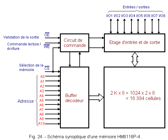
 Click here for the next lesson or in the summary provided for this purpose.
 Top of page
 Next Page