Components with 3 State Outputs (Tri-State) ; Bidirectional Buffer :
In this practice, we will examine the memories. They are of great importance in digital electronics and are widely used in microprocessor systems.
In previous experiments, you have already used various components to store data. The simplest is the toggle that allows you to record a single bit; an example has been given in the previous practice in which a flip-flop was used to retain the restraint.
Since a flip-flop can only store a single bit, when used as a memory, it is said to have a 1 bit capacity.
The shift registers examined above make it possible to record a series of bits the number of which depends on the number of stages.
The flip-flops are also used as dividers, series-parallel or parallel-series converters, or as counting elements.
However, there are components that are only used to store data and that, therefore, take the name of memories.
In the exercises planned in this practice, you will experiment a memory allowing to memorize several thousands of bits.
You know that there are many types of memories, different from one another according to the use for which they are intended. All are characterized by their capacity defined by the number of bits they can contain, by their access time (time required to read or write information).
In addition, there are Random Access Memories (RAM), ROM (Read Only Memories) or Read Only Memory (PROM), Programmable Read Only Memories (RAM) or Programmable Read Only Memory (RAM), only EPROM or UVPROMprogrammable read only memories, erasable by ultraviolet, EAROM or electrically erasable PROM memories.
These memories can be of static or dynamic type and lose information in the absence of power (volatile memories) or keep it (permanent memories).
We will not be able to experience each category of memories ; EPROM for example, require special equipment to be programmed ; the dynamic memories must be generated by so-called "refresh" circuits that are rather complex.
We will use for our experiments a static memory whose capacity is 2 kilobytes or 2 x 8 x 1024 = 16 384 bits exactly.
With this memory, you will use two other integrated circuits ; a twelve-stage counter and a TRI-STATE bidirectional buffer. Since this last component is brand new, before practically verifying its functioning, it is advisable to study it beforehand.
1. - COMPONENTS
WITH OUTPUTS THREE STATES (TRI-STATE)
Figure 1 shows an example of connections made between five components exchanging the data between them.
The arrow indicates in the diagram the meaning of the information (transmitter or receiver).
We can see on this figure the complexity and the anarchic structure of the montage. Indeed, the number of connection conductors grows rapidly with the complexity of the circuit. As you can see in Figure 1, we need 20 drivers for five components.
In general, for a number n of components, a number of links N = n (n - 1) is required.
As a result, the number of drivers increases with the increase in the number of components which increases the cost of the systems in an unacceptable manner.
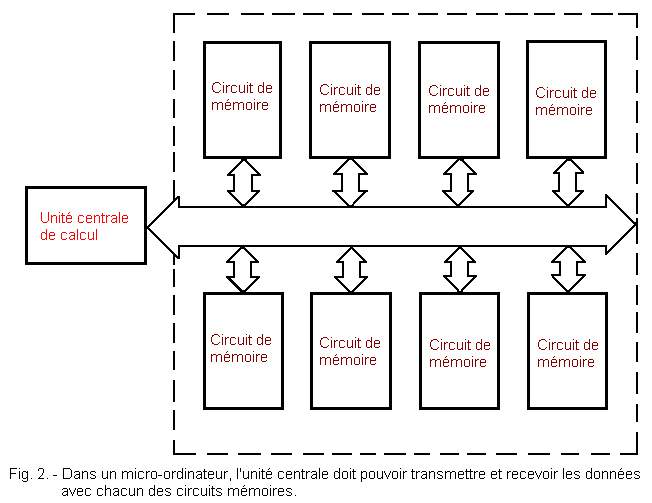
This problem is typical of microcomputer memories in which many integrated memory boxes are used in order to have a large memory.
Each memory circuit contains a portion of the data used by the microcomputer and it is necessary to be able to "read" or "write" this data in a memory independently of the other memories. Usually, it is the central computing unit, that is to say the essential element of the microcomputer that uses these memory boxes and must therefore communicate with each of them.
In this case, the connection between the central unit and each memory circuit requires for the reasons explained above an excessive number of conductors.
This is why, in order to reduce the number of links, it has been imagined another system using only one link to put all the components in communication with each other (Figure 2).
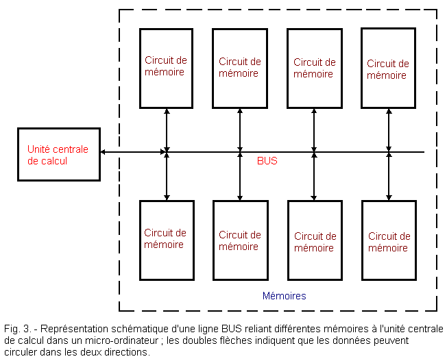
Each of the memory circuits that presents itself to this common line of connection with the central unit can transmit and receive data from one of the other circuits ; this line is usually called in English bus (Figure 3).
On this line, several memory circuits can not transmit data simultaneously ; if several circuits tried to do it, the information would be mixed, which would make them unusable by the receiving circuit. On the other hand, several memory circuits can receive and use the data transmitted by a single transmitter.
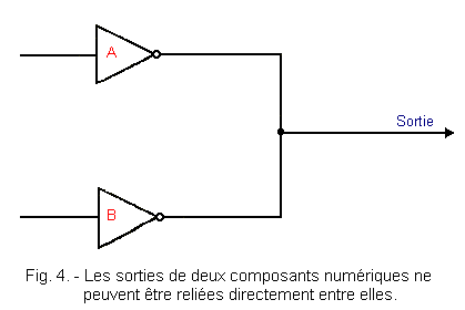
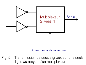
Let's see that it is the technique used to achieve this result. We will assume for the sake of convenience of our study that we want to take with a single driver the levels provided by two inverters.
If we simply realized the parallel connection of the two outputs, as seen in Figure 4, output could not get any useful signal. Indeed, if the output of the inverter A is 1, and the output of the inverter B to 0 for example, the state will be 0 in TTL, and indeterminate but generally taken into account as a 1 (4 V for a 5 V power supply) in MOS technology.
However, there are special components called TRI-STATE, with which it is possible to obtain the same result as with a multiplexer. These components have the particularity of having in addition to a low state and a high state, a so-called "high impedance" state.
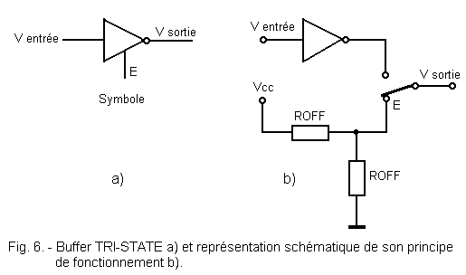
Figure 6-a shows the symbol of a circuit of this type : it is a TRI-STATE inverting buffer which, in addition to the conventional input and output, has a validation input identified in Figure 6-a by the letter E, initial of the English word ENABLE which means precisely valid.
When the level of the input E is high, the component behaves like a normal inverter, that is to say that its output always gives a level complementary to the one applied to its input.
On the other hand, when the level of E is low, the output goes into the state called "high impedance".
Under these conditions, the circuit behaves as if its output was connected to the midpoint of a divider bridge consisting of two resistors of very high values as shown schematically in Figure 6-b.
In practice, when the output of the inverting buffer is in the "high impedance" state, it is virtually isolated from the ground and from the supply voltage.
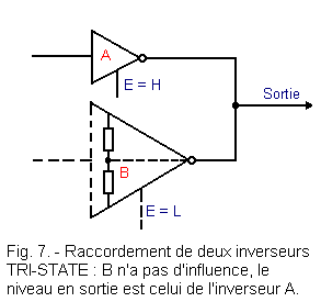
By using reversing buffers of the TRI-STATE type, it is possible to reach the goal that we had previously set for ourselves, namely, connecting the two outputs together as shown in Figure 4; it is sufficient for one of the two inverters to be in the "high impedance" state in order to be able to read the level available at the output of the other inverter TRI-STATE.
By doing so, the signals delivered by each of the TRI-STATE can not overlap or influence each other (Figure 7).
From a structural point of view, a component with three states output is no more complex than a conventional component.
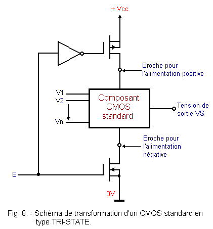
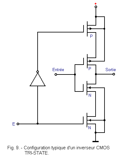
The Figure 8 represents the block diagram of the circuit making it possible to transform a standard CMOS circuit into a TRI-STATE type circuit.
As we can see, it simply includes two MOS transistors connected in series with the two power supply terminals (plus and ground).
When the validation input E is brought to the low level, the two MOS transistors are blocked. They then behave like extremely high resistance values (ROFF = 1012 MΩ) and the CMOS circuit is consequently isolated from the power supply and thus isolated from the other circuits.
In addition to the aforementioned buffers, there are commercially available gates, latches, registers, decoders and multiplexers having a third high impedance state.
In Figure 9, we can see the schematic diagram of a TRI-STATE inverter CMOS type.
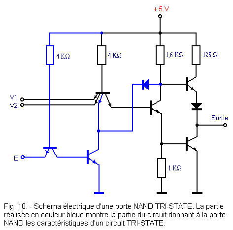
For T.T.L. technology components, the TRI-STATE configuration is different from that of the MOS circuits.
Figure 10 shows the electrical schematic of a NAND T.T.L. door TRI-STATE.
The part of the circuit marked in blue is that which, added to the circuit of the conventional NAND gate, transforms it into a tri-state gate.
When the enable input E is high, the output of the gate goes to the high impedance state, whereas when E is low, it operates normally.
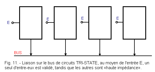
It is very easy with TRI-STATE to constitute circuits around bus lines, it is enough that all the circuits having access to the bus are of type TRI-STATE.
By validating them at the right time, one transmits at a time and the other circuits are in the "high impedance" state (Figure 11).
If, on the other hand, the components used are not of the TRI-STATE type, it is necessary to interpose between them and the bus, buffers of TRI-STATE type.
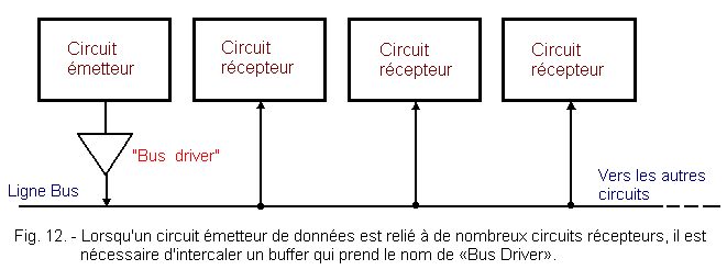
When the output of a circuit must control a large number of other circuits, the useful power of the control signal may be insufficient to ensure proper transmission of the data. This problem can be solved by inserting between the output of the control circuit and the inputs of the controlled circuits a buffer that amplifies the power of the control signal.
In the case where the buffer is connected to the bus, this circuit is called "bus driver circuit" or in English "BUS DRIVER" (Figure 12).
However,
it also happens that a circuit transmitting data must also receive, as we saw earlier in the example of Figure 3.
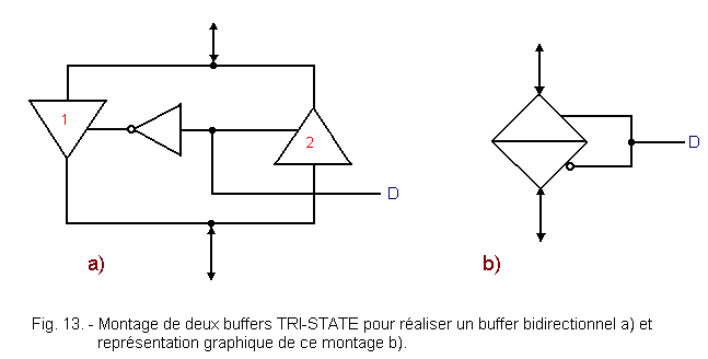
It is therefore necessary that the "bus driver" allows the passage of information in both directions. Components containing two TRI-STATE buffers connected as shown in Figure 13-a are then used.
When the input D (initial direction) is at a low level, the first buffer is validated and the second is "high impedance", the signal can then be routed in the direction from top to bottom.
When against the input D is at a high level, the situation is reversed : the buffer 1 is "high impedance", and the buffer 2 is validated ; the signal can be routed from the bottom up.
Because of this characteristic, this type of buffer is called :"bidirectional buffer" or "bidirectional bus driver" or "transceiver", a term formed by the contraction of the English expression :transmitter-receiver.
For this circuit, the graphical symbol represented in Figure 13-b is sometimes used.
After this theoretical explanation, you can prepare the hardware and perform the first exercise in which you will practically check the operation of the TRI-STATE bidirectional buffer.


 Components with 3 State Outputs (TRI-STATE)
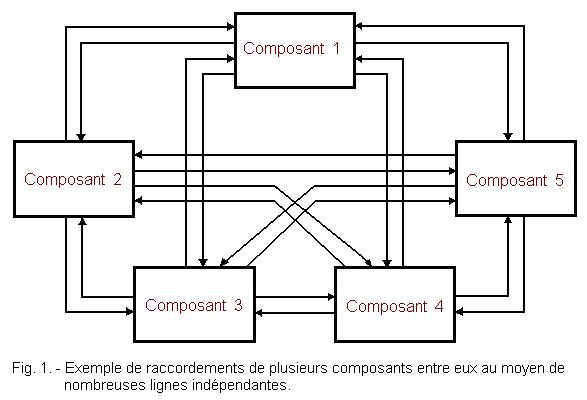
 Click here for the next lesson or in the summary provided for this purpose.
 Top of page
 Next Page