 Slave Master Structure «D» Toggle Slave Master Structure «D» Toggle
|
Functions of the CLEAR and PRESET entries
|
Truth Table and Chronogram
|
|
Application to the Frequency Divider by 2
|
Footer |
Synchronous Flip-flops - Slave Master Structure "D" Toggle - Frequency Divider by 2 :
In this theory, we will examine the operation of two of the most used flip-flops : MASTER SLAVE "D" rocker and MASTER SLAVE "JK" rocker.
These latches have a synchronous operation as we will see now.
1. - SYNCHRONOUS MULTIVIBRATORS
We know that the latch D LATCH type allows through the control input to store a bit of information. This LATCH type D flip-flop operates in asynchronous mode. Indeed, when the control input is at level H, the state of the output follows the state of the input. In other words, as soon as the input changes state, the output also changes state.
However, some digital montages require flip-flops whose outputs switch at a specific time. These flip-flops are synchronous because the taking into account of the information, present on their inputs, is carried out simultaneously during the transition from one logic level to another of the command input. The logical data can be taken into account either on a positive transition (from L to H) or on a negative transition (from H to L) of the control input.
Figure 1-a shows a positive transition (L to H) of a logic signal while Figure 1-b shows a negative transition (H to L) of the signal.
Passages from the high state to the low state and vice versa are not instantaneous as shown in Figures 1-a and 1-b.
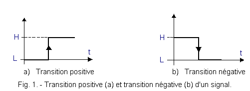
Depending on the technology used, the time taken by a logic signal to switch from one state to the next can vary from less than a nanosecond to several hundred nanoseconds as we have seen in digital technology lessons.
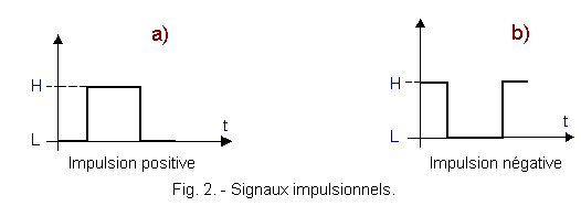
Figure 2-a shows a positive transition of a logic signal followed by a negative transition. This is called a positive impulse.
Figure 2-b represents, for its part, a negative pulse of a logic signal.
The control input of the synchronous flip-flops is called the clock input (in English CLOCK). Indeed, the signal applied to this input is generally provided by a well-defined frequency oscillator. Thus the possible changes of states take place at precise times and regularly spaced in time. The Figure 3 represents a clock signal supplied by a T period oscillator.
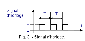
Figure 4 shows the timing diagram of a synchronous flip-flop which stores the data at the time of the positive transition of the clock signal.
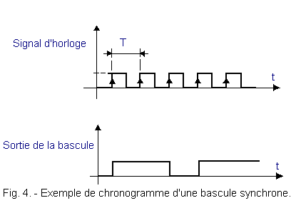
It can be seen that the output does not always change at each positive transition of the clock input. Indeed, a synchronous flip-flop has, in addition to the clock input, one or more information inputs. According to the logical level of these, the rocker switches or remains in the state where it is.
Synchronous flip-flops are designed from asynchronous flip-flops that are associated in the MASTER SLAVE configuration. The first of the synchronous flip-flops is the MASTER SLAVE "D" flip-flop that we are going to examine now.
![]() 2. -
MASTER
STRUCTURE "D" TOGGLE SLAVE
2. -
MASTER
STRUCTURE "D" TOGGLE SLAVE
2. 1. - CONSTITUTION AND FUNCTIONING OF THE MASTER SLAVE "D" ROCKER
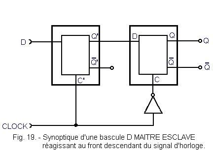
Flip-flop D MASTER SLAVE structure consists of two latches D latch (or latch) placed one after the other. The first is called MASTER, the second is called SLAVE. Figure 5 shows the synoptic of a flip-flop D MASTER SLAVE.
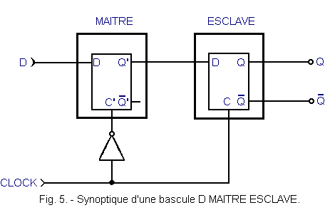
It can be seen that the D input of the SLAVE flip-flop is connected to the Q' output of the MASTER flip-flop. This explains the MASTER and SLAVE denominations assigned to the first and second latch.
Indeed, the input D of the SLAVE copies the output Q' of the MASTER. Any variation of the logical level at the exit of the MASTER is thus found at the entrance of the SLAVE. The SLAVE is well enslaved to the MASTER.
Note that the control inputs of the two flip-flops are always at opposite logical levels. Indeed, an inverter is located between the two validation inputs C' and C.
The command entry that activates the C' and C inputs is called CLOCK IN. Indeed, the rocker examined has a synchronous operation as you will see.
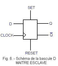
From the outside, the flip-flop D
MASTER SLAVE appears as a flip-flop having a data input D (DATA), a clock input (CLOCK) and two complementary outputs Q and ![]() .
.
If you add a reset input (0) and a SET input (1), the diagram in Figure 6.
Recall the operation of a Multivibrator D latch.
We know that if its control input C is brought to state 1, the output Q copies the input D. If the control input C is set to 0, the output stores the last logical state present on the input just before the negative transition of the command input.
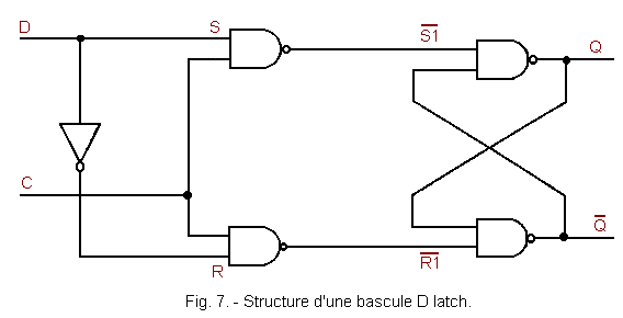
Figure 7 recalls the structure of a latch D latch, while Figure 8 shows the action of the control input C on the outputs Q and ![]() depending on the input D.
depending on the input D.
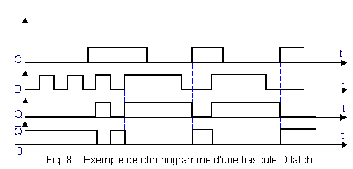
When the output Q copies the input D, the flip-flop D latch is transparent (the logic state of the output Q is the same as that of the input D). When the flip-flop is in the memory position, it is locked (no action of the input D on the output Q).
These two modes of operation (transparency and locking) can be symbolized by a switch that would be controlled by the C input.
The «transparency» mode is illustrated in Figure 9-a, while Figure 9-b shows the «lock» mode.
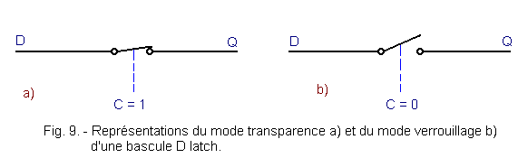
In the «transparency» mode, the closed switch indicates that the output Q follows the input D.
In the «lock» mode, the open switch indicates that the output Q does not follow the input D. The output Q remains in the state where it was just before the negative transition of C.
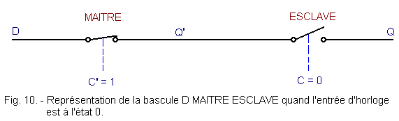
The flip-flop D MASTER SLAVE can be represented by putting in series two switches controlled by the clock input. This representation leads to the diagrams of Figures 10 and 11 according to whether the clock is in state 0 or in state 1.
.gif)
It can be seen that if the clock input of flip-flop D MASTER SLAVE is brought to a stable logic state (0 or 1), the state of input D has no influence on the state of output Q Indeed, to go from D to Q, there is always an open switch.
We will now see that the actual switching of the flip-flop can take place only during the transition from the L level to the H level of the clock.
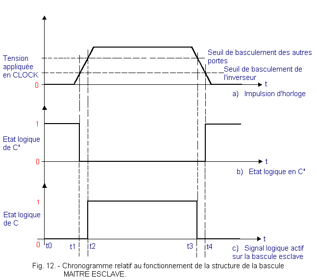
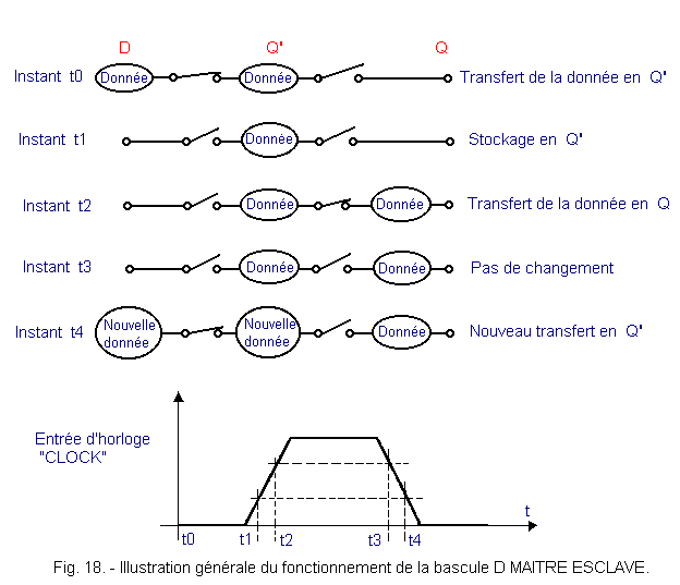
For this, apply to the clock input a voltage pulse whose shape is represented in Figure 12-a. This corresponds to reality as we have seen previously, the rise and fall times of the voltage being never zero.
It must also be taken into account that the inverter disposed between the two control inputs C and C' has a lower switching threshold than that of the other logic gates of the circuit (Figure 12-a).
Figure 12-b shows the logic level thus obtained on the control input C' of the MASTER flip-flop, while Figure 12-c shows the active logic signal on the SLAVE flip-flop.
Let's analyze the action of the clock input on the MASTER rocker and on the SLAVE rocker :
From instant t0 to instant t1, C' = 1 and C = 0. The MASTER is transparent and the SLAVE is locked (see Figure 13).
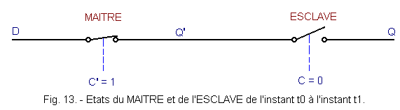
The MASTER toggle transfers the data D at the output Q'. On the other hand, the data Q' is not transferred to the output Q of the flip-flop SLAVE, because the latter is locked.
At time t1, the MASTER is locked and the SLAVE remains locked since C' = 0 and C = 0 (see Figure 14).
The binary information present on the input D just before the instant t1 is stored at the output Q' since C' has passed from the state 1 to the state 0 at the instant t1.
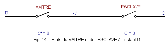
We have stored the data in Q'. Since the SLAVE is still blocked, it has still not been transmitted on the Q output which remains unchanged.
From time t1 to moment t2, nothing changes : the data stored at time t1 is always in Q'.
At time t2, the MASTER is locked and the SLAVE becomes transparent since C' = 0 and C = 1 (see Figure 15).
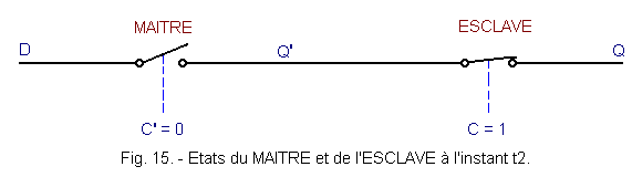
The output Q then copies the input Q'. There is thus switching of the output Q which stores the data present in D at time t1.
It can also be said that the data present at D at time t1 has been transferred to output Q at time t2. The transfer was made on the rising edge of the clock.
From time t2 to time t3, there is no change since C' = 0 and C = 1.
At time t3, the SLAVE is locked, while the MASTER is still locked. Indeed, C' = 0 and C = 0 (see Figure 16. It is noted that the outputs Q' and Q do not change state.
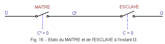
From time t3 to moment t4, the MASTER and the SLAVE are always locked and the outputs Q' and Q retain their logical state.
At time t4, the MASTER becomes transparent since C' = 1 (see Figure 17).
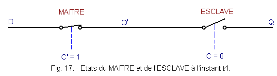
The new data present at D is transferred at the output Q', but not at the output Q since the SLAVE is always locked (C = 0). It can thus be seen that during the negative edge of the clock (from time t3 to time t4), the output Q can not switch.
In summary, the eventual switching of the Q output takes place only at the time of the rising edge of the clock (transition from the L level to the H level of the CLOCK input).
The operation of a Master Slave D flip-flop is synchronous. Its role is to memorize a logical data at a precise moment. This data applied at D is taken into account at the beginning of the rising edge and transferred to the Q output at the end of this rising edge. A new transfer from the D input to the Q output will take place at the next rising edge of the clock.
Between two successive rising edges of the clock, there is no possible change in the Q output.
It should be noted that when the output Q switches, the output ![]() does the same.
does the same.
Figure 18 shows the steps of the flow of the data in the flip-flop D MASTER SLAVE when applying a clock pulse.
Note that if the input of the inverter located between the two control inputs is connected to C' and the output connected to C, the flip-flop D MASTER SLAVE thus constituted takes into account the data present in D at the falling edge of the clock signal. This is the case of the flip-flop shown in Figure 19.
Now let's go back to the detailed structure of a MASTER SLAVE rocker sensitive to the rising edge of the clock.
Replace in Figure 5 each latch D latch by the diagram of the Figure 7.
We come to Figure 20.
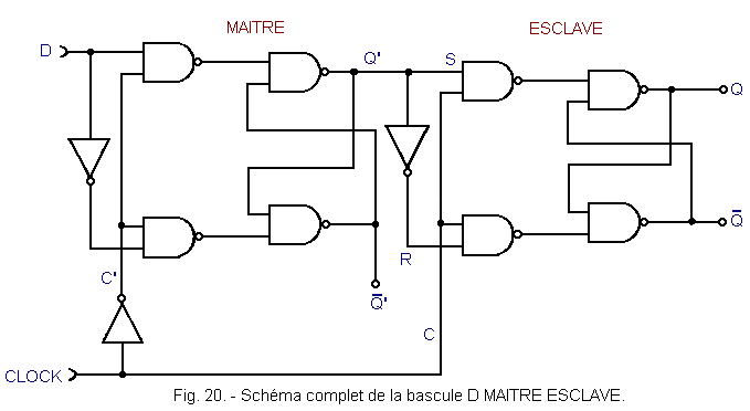
The inverter placed between the inputs S and R of the flip-flop SLAVE can be removed by connecting R to ![]() '.
As a result, the diagram of the MASTER SLAVE flip-flop becomes that of Figure 21.
'.
As a result, the diagram of the MASTER SLAVE flip-flop becomes that of Figure 21.
.gif)
![]() 2. 2. - FUNCTIONS
OF CLEAR AND PRESET INPUTS
2. 2. - FUNCTIONS
OF CLEAR AND PRESET INPUTS
It remains to add to this scheme the reset and reset entries, usually called CLEAR and PRESET. These are connected as shown in Figure 22 which therefore represents the schema of a flip-flop D MASTER SLAVE with the reset and reset entries.
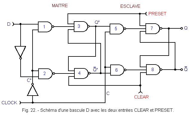
Let's see how the CLEAR and PRESET entries work.
2. 2. 1. - IN A FIRST TIME, CONSIDER THAT THE CLOCK ENTRY IS AT LEVEL L
If the CLOCK input is 0, the SLAVE is locked.
Since the control input C of the slave is set to state 0, the outputs of NAND gates 5 and 6 are in state 1, regardless of the state of D.
The output stage of the flip-flop D, composed of the NAND gates 7 and 8, constitutes a NAND gate RS flip-flop similar to that examined in the previous theory.
The diagrams of Figures 23-a and 23-b are therefore equivalent.
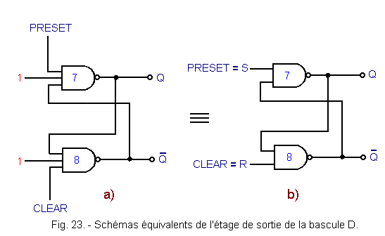
To set flip-flop D to state 1 (Q = 1), set the CLEAR input to state 1 and apply a negative pulse to the PRESET input. This is the reset entry and is active in state 0.
Similarly, to set the flip-flop to 0 (Q = 0), the PRESET input must be set to 1 and a negative pulse must be applied to the CLEAR input. The latter is therefore the reset entry and it is also active in state 0.
If both CLEAR and PRESET inputs are set to 0, the outputs Q and ![]() are forced to state 1. This combination of CLEAR and PRESET entries is rarely used.
are forced to state 1. This combination of CLEAR and PRESET entries is rarely used.
2. 2. 2. - IN A SECOND TIME, CONSIDER THAT CLOCK ENTRANCE IS IN STATE 1
The MASTER is locked since the control input C' is in state 0 and the SLAVE is transparent.
Set the CLEAR input to state 1 and apply a negative pulse to the PRESET input. As can be seen in the Figure 22, this pulse will switch the RS flip-flop composed of the NAND gates 3 and 4 to the state 1 (Q' = 1 and ![]() '
= 0).
'
= 0).
Since the SLAVE is transparent (C = 1), The exits Q and ![]() will copy Q' and
will copy Q' and ![]() '.
The flip-flop D will therefore go to the state 1 (Q = 1 and
'.
The flip-flop D will therefore go to the state 1 (Q = 1 and ![]() = 0).
= 0).
Now set the PRESET input to state 1 and apply a negative pulse to the CLEAR input. This time, the pulse will switch the RS flip-flop to state 0 (Q' = 0 and ![]() '
= 1).
'
= 1).
Since the slave is transparent, the exits Q and ![]() will copy Q' and
will copy Q' and ![]() '.
The flip-flop D will therefore go to the state 0 (Q = 0 and
'.
The flip-flop D will therefore go to the state 0 (Q = 0 and ![]() = 1).
= 1).
Similarly, if the two inputs CLEAR and PRESET are brought to state 0, the outputs Q and ![]() are forced to state 1 by means of the NAND gates 7 and 8. It should be noted that in this case the state of the outputs Q and
are forced to state 1 by means of the NAND gates 7 and 8. It should be noted that in this case the state of the outputs Q and ![]() is identical. We can no longer speak of complementary outputs. This case is very rarely used and some manufacturers even consider it prohibited.
is identical. We can no longer speak of complementary outputs. This case is very rarely used and some manufacturers even consider it prohibited.
Moreover, this state is not stable. It does not persist if the CLEAR and PRESET entries return to their idle state (that is, 1 in our case).
In summary, regardless of the logical state of the inputs D and CLOCK, the entries CLEAR and PRESET are priority and asynchronous, which can be summarized by the truth table of Figure 24. X crosses placed in the boxes D and CLOCK means that the state of these two inputs does not affect the state of the outputs of the flip-flop.
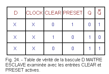
The two inputs CLEAR and PRESET must be in state 1, that is, inactive so that the flip-flop can switch on the active edge of the clock signal.
It should be noted that there are MASTER SLAVE flip-flops whose CLEAR and PRESET inputs are active in state 1. In this case, these two inputs must be brought to state 0 so that the clock signal is active.
Finally, some latches see their two outputs Q and ![]() go to state 0 (and not 1 as in the previous case) when both entries CLEAR and PRESET are both active. All these differences are explained by differences in technological makeup.
go to state 0 (and not 1 as in the previous case) when both entries CLEAR and PRESET are both active. All these differences are explained by differences in technological makeup.
![]() 2. 3. - TABLE OF TRUTH AND CHRONOGRAM
2. 3. - TABLE OF TRUTH AND CHRONOGRAM
The complete functioning of the flip-flop D MASTER SLAVE examined is summarized by the truth table of Figure 25.
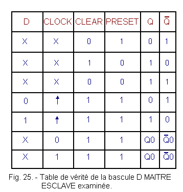
The symbol ![]() that can be seen in the CLOCK column of the truth table indicates a positive transition of the clock signal.
that can be seen in the CLOCK column of the truth table indicates a positive transition of the clock signal.
In this table, the first three lines indicate that the CLEAR and PRESET entries are priority and active on a low level.
The fourth line indicates that the logic state 0 present at D is transferred to the output Q on the rising edge of the clock signal.
The fifth line indicates that the logic state 1 present at D is transferred to the output Q on the rising edge of the clock signal.
In the sixth and seventh lines, Q0 and ![]() 0
are the logical states that the outputs Q and
0
are the logical states that the outputs Q and ![]() took during the last active edge of the clock. These logical states Q0 and
took during the last active edge of the clock. These logical states Q0 and ![]() 0
could be imposed by the priority entries CLEAR and PRESET.
0
could be imposed by the priority entries CLEAR and PRESET.
In other words, these last two lines of the truth table indicate that the outputs Q and ![]() do not switch to a logic level of the clock signal but on a rising edge of this signal.
do not switch to a logic level of the clock signal but on a rising edge of this signal.
Figure 26 shows an example of a timing diagram of the flip-flop D MASTER SLAVE examined.
.gif)
At the beginning of this timeline, the PRESET entry is set to 0, so it is active. The flip-flop is therefore in state 1. Then the PRESET input returns to state 1. The Q output remains set to state 1. The CLEAR input receives a negative impulse which switches the flip-flop to state 0.
The second active edge of the clock has no action on the Q output of the latch since it takes place when the input CLEAR is active, so priority. Then, the entries CLEAR and PRESET become inactive since they are brought to state 1. The flip-flop can now only switch on the positive edge of the clock.
At the third active edge of the clock, the logic state present at D is the state 1. The flip-flop which was in state 0 thus goes to state 1.
When the fourth positive edge occurs, input D is in state 0. The toggle switch therefore switches to state 0.
On the fifth rising edge of the clock, the flip-flop does not change state since D is always in state 0.
Input D goes to state 1 just before the sixth active edge of the clock. As a result, the Q output of the flip-flop goes to state 1 on the sixth rising edge of the clock.
![]() 2. 4. - APPLICATION
TO THE FREQUENCY DIVIDER BY 2
2. 4. - APPLICATION
TO THE FREQUENCY DIVIDER BY 2
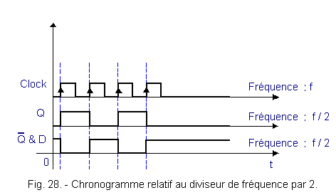
Figure 27 shows the connection to be made to transform a D MASTER SLAVE to a frequency divider by 2.
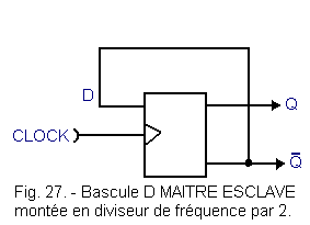
The data D memorized at the output Q during the active edge of the clock is ![]() ,
since
,
since ![]() is connected to D. In other words, whatever the logical state of the output Q before the top of the clock , the flip-flop will go into the complementary logical state during the active clock edge. This mode of operation is called in TOGGLE constructor catalogs.
is connected to D. In other words, whatever the logical state of the output Q before the top of the clock , the flip-flop will go into the complementary logical state during the active clock edge. This mode of operation is called in TOGGLE constructor catalogs.
With the timing diagram of Figure 28, we see that the outputs Q and ![]() are at a frequency half that of the clock input. The 2-fold frequency divider is widely used in electronic meters that will be examined later.
are at a frequency half that of the clock input. The 2-fold frequency divider is widely used in electronic meters that will be examined later.
After the D flip-flop, let's now examine the JK MASTER SLAVE flip-flops.
 Click here for the next lesson or in the summary provided for this purpose. Click here for the next lesson or in the summary provided for this purpose. |
 Top of page Top of page |
|
Previous Page |
 Next Page Next Page |
Nombre de pages vues, à partir de cette date : le 27 Décembre 2019

Envoyez un courrier électronique à Administrateur Web Société pour toute question ou remarque concernant ce site Web.
Version du site : 10. 4. 12 - Site optimisation 1280 x 1024 pixels - Faculté de Nanterre - Dernière modification : 02 Septembre 2016.
Ce site Web a été Créé le, 14 Mars 1999 et ayant Rénové, en Septembre 2016.