 Magnetic Memories Magnetic Memories |
 Magnetic Bubble Memories Magnetic Bubble Memories |
 Footer Footer |
Magnetic Memories - Magnetic Bubble Memories - CCD Memories :
4. - CCD MEMORY
CCD memories are less used than previous memories. The abbreviation is formed from the initials of Charge Coupled Device (dispositif à couple de charge).
These are devices in MOS technology consisting of numerous capacitive cells connected in series so as to form dynamic type shift registers, similar to those described in theory 8.
Figure 51 shows the block diagram of a CCD memory with a capacity of 16 384 bits.
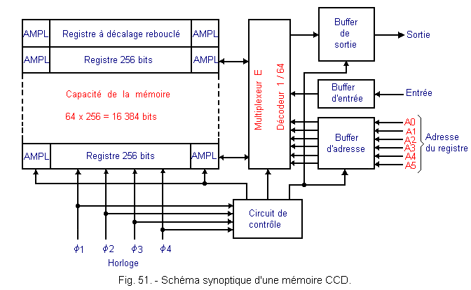
The memory consists of 64 registers that are looped back on themselves, each consisting of 256 cells, so able to hold 256 bits.
The amplifiers that precede and follow each register have the task of regenerating the cell charges.
Only one register can be accessed at a time and the desired register is selected by sending a 6-bit address 6 bits (26 = 64).
The stages of the registers contain the data in the form of charges, materialization already encountered in the dynamic RAM.
In this case too, the loads must be periodically refreshed and the data is constantly moving.
This is ensured by the four clock signals designated f1, f2, f3 and f4.
The advantages offered by CCD are : large capacity and relatively low cost.
The access time of these memories is high ; because, because of their structure, it is necessary, to read or write a bit, for example, to select the register that contains it and then to wait for the bit as it flows, to reach the output of the register.
Remember that RAM, like ROM, are random access memories, that is, the time required for the read or write operation is independent of the physical position, in the matrix of the memory of the cell to which one wants to access.
The CCD memories are on the other hand with serial access, the time taken by the bits to be transferred from one cell to the next is approximately that of a cycle in a random access memory.
As a result, the access time of a serial memory with 256 bits per register (as in the previous example) is 256 times the cycle time of a random access memory.
For this reason, CCD are not able to compete with RAM, but can be considered high-capacity replacement memories for computers ; in this case, they are called mass memories.
![]() 5. - MAGNETIC MEMORY
5. - MAGNETIC MEMORY
They are of two types : memories with cores, old, and memories with bubbles which are called to a brilliant future.
5. 1. - MEMORIES AT TORES OF FERRITE
These no volatile RAM memories have been widely used ; but the complexity of their manufacture, their cost and their size gradually made them give up.
5. 1. 1. - PRINCIPLE
Some ferrites of copper and manganese (ferroxcube) have two very interesting characteristics. Their coercive field (Hc), that is to say the field for which the magnetization is canceled, is very weak. On the other hand, the hysteresis cycle of these ferrites is almost rectangular (Figure 52-a).
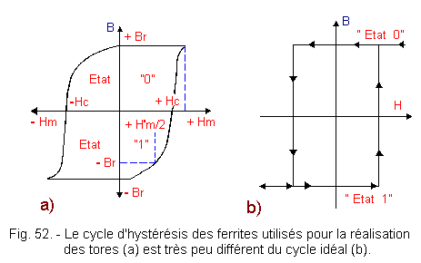
So just take logical conventions :
Writing : The state 0 will be given by the direction of the magnetic field generated by a current flowing in the direction of the arrow drawn on the winding L1 of Figure 53 and consequently the residual induction + Br resulting from this field. The torus will be in state 1 when the direction of the induction will be the opposite of that necessary to produce the state 0.
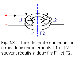
Reading : Let the winding L1 travel through a current I. This current produces a magnetic field. Depending on the initial state of magnetization of the torus, two things can happen :
![]() If the torus was originally in the state of remanent induction + Br (state 0) its permeability is low and, if the hysteresis cycle of the ferrite is perfectly rectangular, as represented in Figure 52-b, we will not collect no voltage across the winding L2.
If the torus was originally in the state of remanent induction + Br (state 0) its permeability is low and, if the hysteresis cycle of the ferrite is perfectly rectangular, as represented in Figure 52-b, we will not collect no voltage across the winding L2.
![]() If, on the other hand, the initial state of the torus was at state 1, the induced field, if it has a value at least equal to Hm, causes the magnetic state of this torus to switch to state 0. In doing so, the operating point will pass through a zone of high permeability of the characteristic of the ferrite, from which a flow variation will result which will generate an electromotive force across the winding L2.
If, on the other hand, the initial state of the torus was at state 1, the induced field, if it has a value at least equal to Hm, causes the magnetic state of this torus to switch to state 0. In doing so, the operating point will pass through a zone of high permeability of the characteristic of the ferrite, from which a flow variation will result which will generate an electromotive force across the winding L2.
5. 1. 2. - CONNECTIONS AND USE
We have seen that to switch a rectangular hysteresis ring magnetic torus from state 0 (+ Br) to state 1 (- Br), a field or a magnetomotive force of at least Hm is required.
If to produce a field Hm, it is necessary a current Im traversing a wire, it will be necessary if one uses two windings, two currents Im / 2 of the same direction. In this way, the tilt of the toroid will only be obtained if the two windings are fed simultaneously by a current pulse Im / 2.
This principle of coincidence of currents is that used in magnetic memories.
The diagram of Figure 54 shows the structure of a ferrite core memory. There is a 9-core matrix of ferrite. In reality, these memories include thousands.
This system allows you to memorize 9 bits.
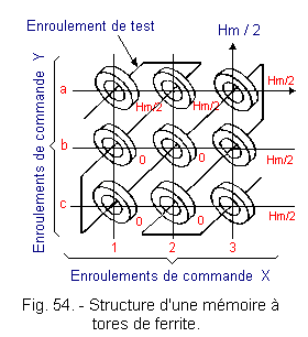
The tori are arranged in rows and columns. To access one of these tori for reading or writing, a pulse is simultaneously sent on the rows (Y) and on the columns (X).
Take for example the torus at the intersection of row b and column 2. Suppose that initially all the tori of the matrix are in state 0. If we send at once in both wires a current pulse at least equal to Im, the torus switches to state 1. If we now run the same two wires by a current in the opposite direction, the torus will go back to state 0 and the test wire which crosses all the tori of the matrix will be the seat of a pulse resulting from the reading of the information contained in memory.
We see that the reading of the memory is destructive, that is to say that the information is lost after each reading ; it is therefore necessary in this technology, to rewrite the information after each reading.
In the systems proposed by the manufacturers, instead of reversing the direction of the pulses in a pair of wires for reading and writing the information, two vertical wires and two horizontal wires fed in the opposite direction are used. One pair is specialized for writing and the other for reading. To rewrite the information after reading, it is therefore sufficient to reinject on the writing son an impulse slightly delayed compared to the reading.
Figure 55 shows the block diagram of such a rewrite device.
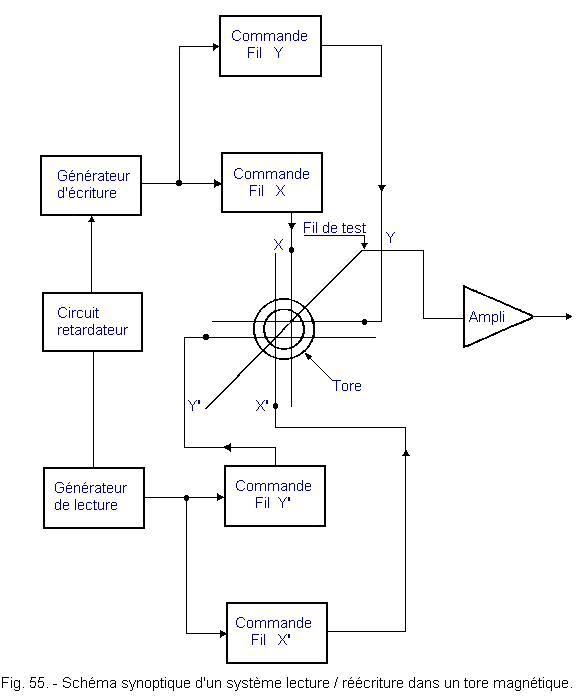
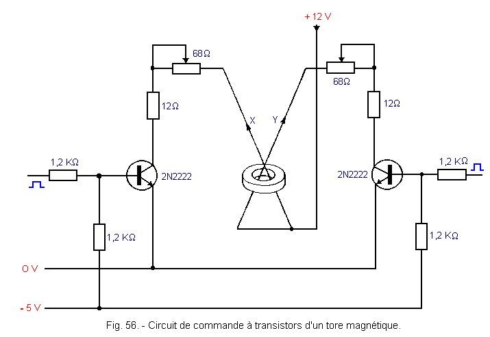
Figure 56 gives an example of transistor core control circuitry as used.
![]() 5. 2. - MAGNETIC BUBBLE
MEMORY
5. 2. - MAGNETIC BUBBLE
MEMORY
Magnetic bubble memories are, like CCD, serial access memories.
5. 2. 1. - MAGNETIC BUBBLE
In magnetic thin-layer material, the magnetized zones take on any shape and are distributed randomly ; however, if an increasing perpendicular external magnetic field is applied, these areas shrink to form tiny cylinders (Figure 57).
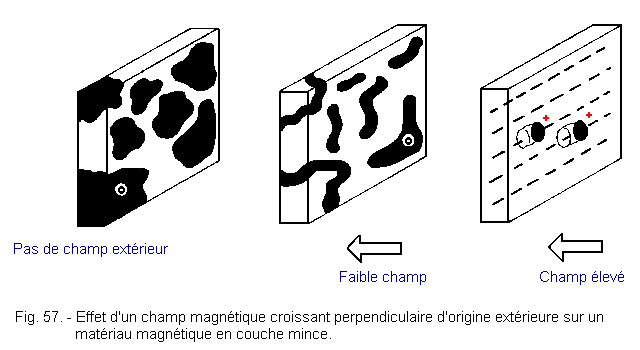
These cylinders, which are broken by a reverse magnetic field, constitute «magnetic bubbles» and can be used to memorize information.
5. 2. 2. - DESCRIPTION OF BUBBLE MEMORIES
Figure 58 shows a bubble memory seen in section.

The 2 µm diameter bubbles circulate in the thin magnetic layer (2 to 3 µm) deposited on a no magnetic substrate (generally a gadolinium yttrium garnet or glass).
The permanent external magnetic field, perpendicular to the plane of memory, is essential for the existence of bubbles. It is provided by a set of permanent magnets.
A rotating magnetic field is provided by two small orthogonal windings made of aluminum wires. This magnetic field rotating very low relative to the permanent magnetic field, called stabilization, allows to circulate the bubbles (Figure 59).
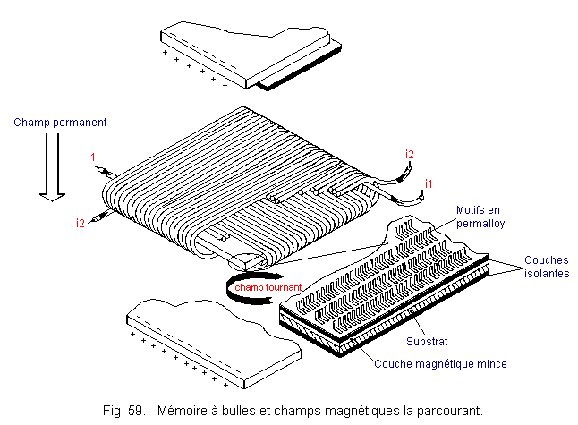
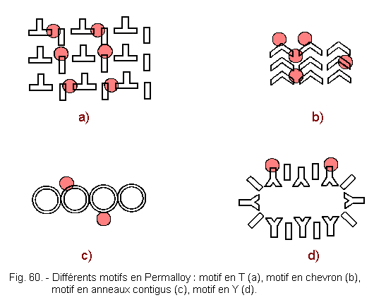
The bubbles are guided in their movements by a Permalloy guide whose patterns vary according to the manufacturers (Figure 60).
5. 2. 3. - OPERATION OF BUBBLE MEMORY
A bubble memory consists of a kind of shift register looped back on itself in which a bubble represents a bit 1 and its absence, a bit 0.
To write in memory, it will therefore create bubbles.
To read, it will detect the presence of bubbles. But it will be necessary to wait for the bubbles corresponding to the chosen address to scroll through the bubble detector because of the sequential access of the memory, hence the need to circulate them.
We do all this by organizing different paths in rings or loops thanks to Permalloy guides.
Figure 61 shows the organization of a bubble memory.
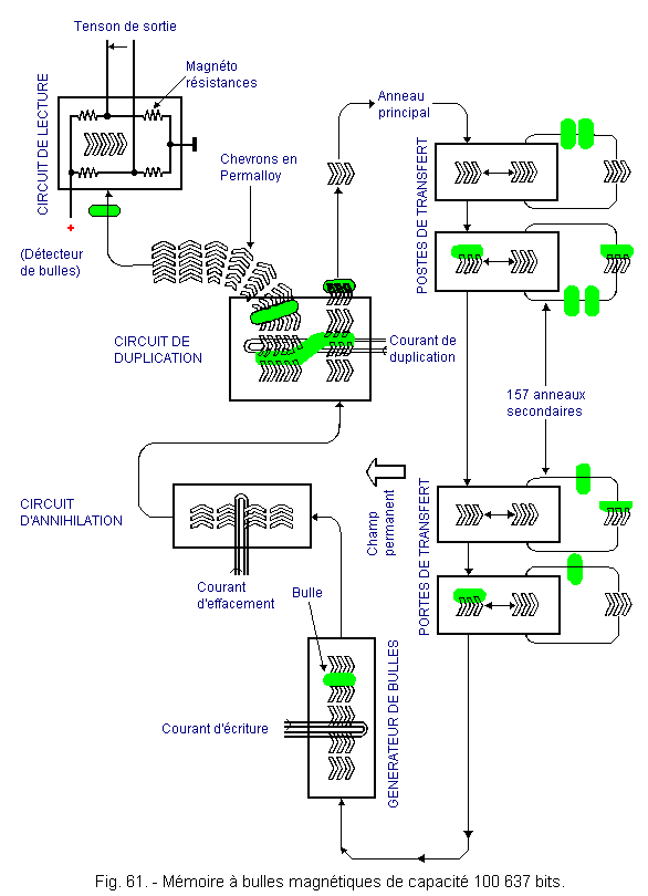
In order to increase the capacity of these memories, secondary rings are added to the main ring which are small ring registers in which the bubbles circulate.
To read the memory, it will be necessary to select the secondary ring, to transfer the data of this one in the main ring then to read the data in series.
We see in Figure 61 that it is necessary to read information to duplicate the bubble.
Indeed, reading is destructive, it makes through a suitable circuit a double of it and it is this new bubble that passes into the reading circuit while the original continues to rotate in the main loop.
Detection of the bubble itself is done by means of a bridge of magneto-resistors. The bubble, passing on a magneto-resistance, then produces a voltage pulse.
The transfer of the bubble from a secondary loop to the main loop is achieved through a specialized circuit called transfer station and whose principle resembles that of the duplication circuit.
5. 2. 4. - PROPERTIES OF BUBBLE MEMORIES
Magnetic bubble memories have the advantage of having a large capacity (of the order of a million bits) in a small volume but have a high access time (10 to 50 ms).
They are expected to replace magnetic disk mass memories because of their high reliability, low weight and limited volume.
The memory given as an example in Figure 61 comprises 157 secondary loops of 641 bubbles each, see 100 637 bits.
Some memories include several main loops, they are said to have several pages.
The commercially available bubble memories are packaged in cassettes comprising all the circuits necessary for their operation. Their capacity varies from 60K bytes to 4M bytes, their access time is a few tens of ms.
With the bubble memories, this panorama of memories ends. In the next theory 13, you will be able to see the programmable logic networks which, in some cases, can advantageously replace the ROM because they are less expensive.
 Click here for the next lesson or in the summary provided for this purpose. Click here for the next lesson or in the summary provided for this purpose. |
|
 Previous Page Previous Page |
 Next Page Next Page |
Nombre de pages vues, à partir de cette date : le 27 Décembre 2019
Envoyez un courrier électronique à Administrateur Web Société pour toute question ou remarque concernant ce site Web.
Version du site : 10. 4. 12 - Site optimisation 1280 x 1024 pixels - Faculté de Nanterre - Dernière modification : 02 Septembre 2016.
Ce site Web a été Créé le, 14 Mars 1999 et ayant Rénové, en Septembre 2016.
